- ID METAL
- 070-7014-1011
- id@idmetal.co.kr

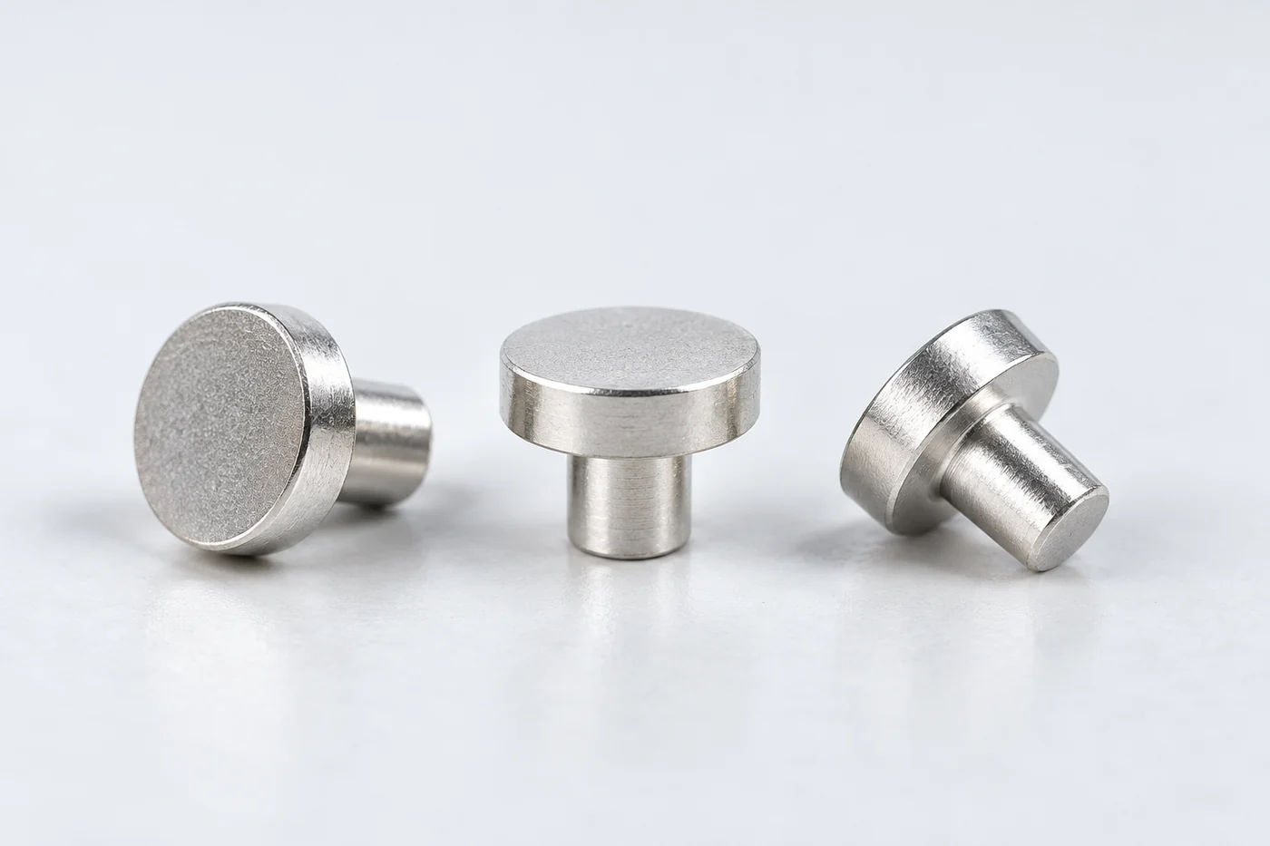
AgNi와 AgCu 전기접점은 겉으로 비슷해 보여도 내부 조직과 표면에서 일어나는 현상이 다릅니다. 은-니켈의 분산 조직, 은-구리의 합금 상태, 가공과 열 이력은 접촉저항·마모·아크 침식·융착에 서로 다른 영향을 줍니다.
재질 선택의 출발점은 은 함량이나 경도 순위가 아니라 실제 접점의 역할입니다. 전류를 오래 흘리는지, 반복해서 끊는지, 상대면을 미끄러지는지에 따라 필요한 성질이 달라집니다. 세부 등급과 공급 상태를 구분하고, 접촉력·표면·접합을 포함한 완성품 조건에서 비교해야 합니다.
재료와 조직
AgNi의 Ni 분산과 AgCu의 합금 상태를 구분합니다.
접촉과 개폐
전도율·표면막·접촉력·아크 손상을 연결합니다.
제조와 검증
성형·접합·시험·도면으로 재질 선정을 구체화합니다.
개폐용 전기접점은 닫힌 상태에서 전류를 전달하고, 열리는 순간에는 전류를 끊어야 합니다. 이 두 조건이 재료에 요구하는 성질은 같지 않습니다. 낮은 전기저항에 유리한 은도 반복되는 충돌·미끄럼·아크에서는 변형, 마모, 재료 전이와 융착을 겪을 수 있습니다.
AgNi는 은 속에 니켈을 분산시켜 접촉면의 내구 거동을 조절하는 재료군이며, AgCu는 은에 구리를 합금화해 기계적 성질과 전기적 성질을 조정하는 재료군입니다. 어느 쪽이 우수한지는 합금 이름보다 접점의 실제 역할에 달려 있습니다. 통전, 개폐, 미끄럼 접촉을 먼저 구분해야 비교가 성립합니다.
| 구분 | AgNi | AgCu |
|---|---|---|
| 금속 조직의 핵심 | 은 기지와 별도의 니켈상 | Ag-rich상과 Cu-rich상, 상태에 따른 고용·석출 |
| 주요 검토 항목 | 니켈 함량·분포·조직 방향·밀도 | 구리 함량·조질·열 이력·표면 산화 |
| 접점 성능의 확인 | 접촉저항·침식·융착·재료 전이 | 접촉저항·마모·산화·재료 전이 |
| 재질명만으로 알 수 없는 것 | 허용 전류, 수명, 실제 접촉력 | 허용 전류, 수명, 실제 접촉력 |
은계 접점 머리와 동계 캐리어는 다른 역할을 합니다. 접점 머리는 상대 접점과 맞닿는 표면을 제공하고, 캐리어는 전류 경로와 기계적 지지 또는 탄성 기능을 맡습니다. 캐리어가 동이라는 이유로 조립품 전체를 AgCu 합금이라고 부르면 접점 재질과 구조를 혼동하게 됩니다.
비교 대상을 정할 때는 접점 머리의 조성, 단일재·복합재 구조, 상대 접점 재질, 접촉 형상을 함께 고정합니다. AgNi 접점에 큰 하중을 주고 AgCu 접점에는 작은 하중을 준 시험은 재질 효과만 비교한 시험이 아닙니다. 동일한 완성품 조건에서 재질을 바꾸거나, 재질에 맞게 설계를 조정했다면 그 변경까지 기록해야 합니다.
본문의 사진은 접점 형상과 조립 관계를 설명하기 위해 생성한 이미지입니다. 실제 납품품의 성분·치수·검사 결과를 나타내지 않습니다. 움직이는 단면 역시 재료와 전류 경로를 이해하기 위한 설명 모델이며, 특정 제품의 현미경 조직이나 수명 예측 결과는 아닙니다.
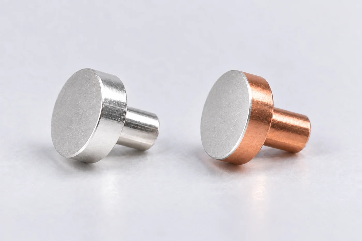
은과 니켈은 고체 상태에서 서로 거의 녹아들지 않으며, 액상에서도 상호 용해가 제한됩니다. 따라서 일반적인 고니켈 AgNi 접점재는 두 금속을 균일한 단일상으로 만드는 대신, 은 기지 안에 니켈상을 분산시킵니다. 은이 전류와 열의 통로를 제공하고, 니켈상의 분포와 형태가 접촉면의 변형·침식 거동에 관여합니다.
AgNi10·AgNi15·AgNi20의 숫자는 통상 니켈의 질량 백분율을 나타냅니다. 이는 현미경 사진에서 보이는 면적 비율이나 체적 비율과 같은 값이 아닙니다. 성적서에는 공칭 기호와 실제 성분 허용 범위를 함께 확인하고, 복합 리벳이라면 접점층의 조성과 지지부 조성을 따로 표시해야 합니다.
| 재료군 | 조직·제조 관점 | 선정 시 주의점 |
|---|---|---|
| AgNi0.15 | 소량의 Ni로 은의 결정립 성장 억제 | AgNi10의 묽은 버전처럼 성능을 환산하지 않습니다. |
| AgNi10·15·20 | 은 기지 안의 Ni분산, 통상 분말야금 경로 | 함량뿐 아니라 분산·밀도·조질을 확인합니다. |
| AgNi30·40 | Ni 비율이 더 높은 복합 조직 | 저항·성형성과 필요한 접촉력을 함께 검토합니다. |
분말 혼합·성형·소결 뒤 압출과 신선을 거치면 니켈 입자가 가공 방향으로 길어질 수 있습니다. 같은 소재도 종단면에서는 섬유처럼, 횡단면에서는 분리된 입자처럼 보일 수 있습니다. 조직 판독에서는 관찰 방향을 기록해야 하며, 서로 다른 절단면을 보고 분산 품질이 다르다고 단정해서는 안 됩니다.
니켈을 늘리면 성분만 바뀌는 것이 아니라 전류가 흐르는 은의 연속 경로, 경도, 변형 능력도 함께 달라집니다. 니켈 함량이 높은 등급은 특정 개폐 조건에서 유리할 수 있지만, 그 장점을 얻으려면 접촉력과 구동 구조가 뒷받침되어야 합니다. 니켈 함량을 높이는 것만으로 모든 부하의 수명이 길어지는 것은 아닙니다.
조직 비교 화면에서는 은 기지와 분산상의 연결 관계를 확인하면 됩니다. 입자 크기나 간격을 화면에서 재어 실제 제조 규격으로 사용할 수는 없습니다. 실제 재료의 균일성은 정해진 위치의 금속조직 관찰, 성분 분석, 밀도와 물성 결과를 연결해 판단합니다.
AgCu에서는 구리가 은 안에 고용될 수 있지만, 고체 상태의 용해도에는 한계가 있습니다. 온도와 조성에 따라 Ag-rich상과 Cu-rich상이 함께 존재하며, 냉각 속도와 후속 열처리에 따라 그 크기와 분포가 바뀝니다. 따라서 AgCu를 은 전체에 구리가 항상 균일하게 녹아 있는 금속이라고 설명하면 실제 조직을 놓치게 됩니다.
AgCu3와 AgCu10은 모두 은-구리계이지만 구리 함량과 공급 상태가 다릅니다. 구리 첨가는 순은의 기계적 강도를 높이는 데 사용되며, 냉간 가공도 경도를 변화시킵니다. 용체화·냉각·시효에 따른 석출 거동이 가능한 조성이라도, 납품 상태가 실제로 시효경화재인지 별도로 확인해야 합니다.
| 표기·구조 | 의미 | 도면에서 필요한 정보 |
|---|---|---|
| AgCu10 | 통상 Cu 약 10질량%의 은-구리 합금 | 성분 범위와 공급 조질 |
| Ag/Cu 층상 구조 | 은층과 동층을 접합한 복합 구조 | 각 층의 재질·두께·계면 품질 |
| AgNi/Cu 복합 접점 | AgNi 접점층과 Cu 지지부 | 접촉층 조성, 잔여 두께, 접합 상태 |
| 은도금 동 | 동 모재 표면에 형성한 은도금층 | 도금 두께·기공·접착·마모 조건 |
슬래시 표기는 공급사와 문헌의 관행에 따라 다릅니다. 예를 들어 Ag/Ni는 층상 구조가 아니라 니켈 분산 복합재를 뜻하기도 합니다. 기호만으로 구조를 확정하지 말고 재료 설명과 단면도에서 합금·분산 복합·클래드·도금을 구분합니다.
NIST의 Ag-Cu 평형 계산은 공정 반응을 약 779°C, 액상 조성을 약 28.4질량% Cu로 제시합니다. 이 값은 AgCu3·AgCu10의 모든 부분이 같은 온도에서 동시에 녹는다는 뜻이 아닙니다. 합금 조성별 고상선·액상선과 실제 열 이력을 보아야 하며, 공정 온도를 접점의 허용 사용 온도로 해석해서도 안 됩니다.
공급사의 AgCu3 자료에는 시효경화 가능 여부가 “아니오”로 표시된 사례가 있습니다. 그러므로 “AgCu는 모두 시효경화로 강해집니다”라는 설명은 적절하지 않습니다. 실제 공정에서는 냉간 가공으로 얻은 경도가 브레이징이나 어닐링 뒤 얼마나 유지되는지, 최종 접점의 경도와 변형량으로 확인하는 편이 유용합니다.
구리 함량이 커질수록 기계적 성질의 이점과 표면 산화에 대한 부담을 함께 보아야 합니다. 재료 내부의 구리상은 강도와 마모에 관여하지만, 접촉면에 형성된 산화물은 전류가 통과하는 계면을 바꿉니다. 같은 AgCu라도 연속 미끄럼으로 표면이 갱신되는 접점과 장기간 닫히지 않는 저하중 접점은 다른 평가가 필요합니다.
AgNi의 분산상 구조 ≠ AgCu의 합금 조직
Ag 기지 속에 Ni 상이 분산된 복합재 개념입니다. 길쭉한 표시는 압출 등에 따른 배향을 설명하기 위한 것이며, 모든 제품의 입자 형상이나 조직을 대표하지 않습니다.
색과 영역의 크기·개수는 상을 구분하기 위한 설명 요소입니다. 현미경 사진, 실측 입도, 함량비 또는 제조 조직의 재현이 아닙니다. AgCu를 Ni 입자와 동일한 방식으로 혼합한 재료라는 뜻도 아닙니다. 합금명만으로 접촉저항·내아크성·수명을 계산할 수 없으며, 조성 및 제조 이력과 실제 접점 시험을 함께 확인해야 합니다.
전도율 표는 재질의 차이를 읽는 출발점이지만, 접점 수명표는 아닙니다. 아래는 Heraeus의 공개 재료표에 제시된 범위를 같은 공급사 기준으로 옮긴 예시입니다. 제품 형태와 조질이 하나로 통일된 비교시험은 아니며, 전도율과 경도 범위의 양 끝값이 같은 시편 상태를 의미하지도 않습니다.
| 공개 등급 | 전도율, %IACS | 비커스 경도, HV | 자료의 성격 |
|---|---|---|---|
| AgCu3 / Hera 343 | 90.53–95.56 | 45–95 | 공개 물성 범위 |
| AgCu10 / Hera 342 | 81.9–86 | 65–120 | 공개 물성 범위 |
| AgNi10 / Hera 367 | 81.9–86 | 50–90 | 조질에 따른 범위 |
| AgNi20 / Hera 365 | 74.78–78.18 | 60–110 | 공개 물성 범위 |
IACS는 국제적으로 사용하는 전기전도율의 기준입니다. 100% IACS는 20°C에서 약 58 MS/m에 해당하며, %IACS는 은 함량이 아닙니다. 표의 전도율 항목에는 개별 측정 온도가 별도로 명시되지 않았으므로 이를 임의의 고온 조건으로 확대 적용할 수 없습니다. 실제 구매에서는 측정 온도·방법과 보증 범위를 확인합니다.
이 표에서 AgNi10과 AgCu10의 전도율 범위는 같습니다. 따라서 “니켈이 들어가면 AgCu보다 항상 전기가 덜 통합니다”라고 순위를 매길 근거는 없습니다. 다른 제조사의 같은 공칭 등급이 다른 참고값을 제시하기도 합니다. 서로 다른 공급사의 최대값과 최소값을 섞어 하나의 대표값으로 만들면 공정·조직·상태 차이가 사라집니다.
경도 역시 시험 하중과 측정 위치가 중요합니다. HV1과 HV10처럼 하중이 다른 결과, 얇은 접점층과 충분히 두꺼운 소재의 결과를 그대로 비교하지 않습니다. 접점층 아래의 지지재나 가장자리, 압흔 간격이 측정에 영향을 주지 않도록 시험 조건을 정해야 합니다.
예를 들어 같은 AgCu20 공개 자료에서도 어닐링 상태의 경도는 80–120 HV, 가공경화 상태는 130–190 HV로 구분됩니다. 이 차이는 합금명을 그대로 유지해도 변형 이력이 물성을 바꾼다는 뜻입니다. 필요한 경도는 최종 열처리와 접합 뒤의 상태로 지정하고, 그 경도가 접촉저항과 균열에 미치는 영향까지 검증해야 합니다.
두 접점이 닿아 보여도 명목상 접촉면 전체가 금속끼리 맞닿는 것은 아닙니다. 미세한 돌기 중 일부가 접촉점을 만들고, 전류는 그 좁은 영역으로 모여 흐릅니다. 이때 생기는 집중저항과 표면막의 영향은 재료 내부의 벌크저항과 구분해야 합니다.
접촉력은 이 실제 접촉 영역을 바꿉니다. 더 단단한 재료가 마모에는 유리하더라도 같은 하중에서 접촉 영역이 충분히 형성되지 않으면 계면저항이 커질 수 있습니다. 힘을 높이는 방안도 구동력, 스프링 응력, 충돌과 마모를 함께 바꾸므로 재질 선택과 기구 설계를 분리할 수 없습니다.
| 저항의 위치 | 주요 영향 인자 | 분리해서 확인할 방법 |
|---|---|---|
| 소재 내부 | 전도율·길이·단면·온도 | 치수를 정한 시편 또는 도체 구간 측정 |
| 접점-접점 계면 | 실접촉 면적·하중·표면막 | 접촉력을 제어한 4단자 측정 |
| 접점-캐리어 접합부 | 접합 면적·산화·공극·체결 상태 | 전압 검출점을 접합부 양측에 배치 |
| 조립품 전체 | 각 저항과 열 경로의 합 | 실제 장착 조건의 전압강하·온도상승 |
설명용으로 접촉부 저항을 1 mΩ로 고정하면, 10 A 통전 시 손실은 0.1 W, 30 A에서는 0.9 W입니다. 전류가 세 배가 되면 같은 저항에서 손실은 아홉 배가 됩니다. 이 계산은 발열 전력의 예시이며, 실제 온도상승은 캐리어·단자·주변 공기와 열이 이동하는 경로까지 알아야 구할 수 있습니다.
AgNi와 AgCu 비교에서도 최초의 낮은 저항 하나보다 반복 작동 뒤의 분포가 중요합니다. 평균은 낮아도 간헐적인 큰 전압강하가 생기면 신호 전달에 문제가 될 수 있습니다. 통전 부품에서는 안정화된 온도와 저항을 함께 기록해, 재질 문제인지 하중 저하나 접합부 문제인지 구분합니다.
저항 설명 모델에서는 전류 경로와 계면의 위치를 나누어 확인할 수 있습니다. 모델의 단순화된 접촉점이나 조절값은 실제 표면 거칠기·산화막 두께·합금 등급을 재현하지 않습니다. 실제 재료 비교에는 동일한 접촉력과 표면 상태로 얻은 측정값을 사용해야 합니다.
Rb = ρL/A · R = Rb + Rc · V = IR · P = I²R
등가 벌크 경로의 전체 길이 L=20 mm, 단면적 A=4 mm²를 가정하고 한 곳의 접촉 계면 저항 Rc를 직렬로 더합니다. 별도 접합부의 저항은 포함하지 않습니다. ρ와 Rc는 서로 독립적인 예제 입력값이며 AgNi·AgCu의 대표값이나 시험 결과가 아닙니다. 3D는 계면 위치를 설명하며 실제 리벳 형상으로부터 저항을 해석하지 않습니다. 파란 선은 계면 위치 표식이고 절연막이나 틈이 아닙니다. 비저항은 일정하다고 가정합니다. 열전달·온도 상승·접촉압력·수축저항의 미세기구·산화막 변화·개폐 아크·수명은 계산하지 않습니다. 0 A에서는 손실이 0이며 아래 색 막대는 저항의 비율을 나타냅니다.
접점이 분리될 때 전류가 즉시 사라지지 않으면 좁은 간극에 아크가 형성될 수 있습니다. 국부적인 용융과 증발, 용융 금속의 이동이 반복되면 접점 표면에 크레이터와 돌기가 생깁니다. 접점이 닫힐 때의 바운스도 짧은 개방과 재접촉을 반복해 국부 손상을 만들 수 있습니다.
AgNi의 별도 니켈상은 은만 있는 조직과 다른 침식·전이 거동을 만듭니다. 그러나 AgNi가 아크에 녹지 않는 재료라는 뜻은 아닙니다. 입자 분산, 공극, 접점 크기와 상대 재질, 아크의 체류 위치에 따라 손상 형태가 바뀌므로 함량과 조직을 함께 다루어야 합니다.
AgNi를 검토하는 이유는 전도율의 최고값보다 은의 전도성과 분산상이 제공하는 침식·전이 억제 효과를 함께 활용하려는 데 있습니다. 공급사 기술자료는 적용되는 개폐 조건에서 은과 은합금 대비 개선된 내침식성을 설명합니다. 다만 AgCu의 모든 등급과 모든 회로에서 우월하다는 의미는 아니므로, 낮은 저항 유지와 융착 억제 사이의 균형을 실제 부하에서 확인합니다.
| 현상 | 관찰할 결과 | 함께 기록할 작동 조건 |
|---|---|---|
| 아크 침식 | 질량 변화·깊이·체적 손실·거칠기 | 전압·전류 파형, 아크 지속시간 |
| 융착 | 개방 실패·분리력·발생 빈도 | 투입 전류·바운스·개방 기구 |
| 재료 전이 | 한쪽 돌기와 상대쪽 크레이터 | DC 극성, 부하 종류, 개폐 속도 |
| 표면막 증가 | 저항 분포·표면 성분 변화 | 분위기·정지 시간·접촉력 |
AgCu의 구리 첨가도 순은 대비 강도와 침식·전이 특성을 바꿉니다. 다만 구리 함량 증가에 따른 표면 산화가 반복 개폐 후 저항에 불리하게 작용할 수 있습니다. AgNi와 AgCu의 비교는 “내아크성” 한 칸으로 끝내지 말고, 침식량·융착·저항 상승 중 실제 고장 기준에 직접 연결되는 항목을 분리해야 합니다.
AC의 전류 영점, DC의 극성, 유도성 부하의 저장 에너지, 용량성 부하의 투입 전류는 서로 다른 조건입니다. 따라서 공급사 자료에 나타난 사용 전류 예시를 접점 소재의 보편적인 정격으로 옮겨 쓰면 안 됩니다. 동일 전류라도 전원 임피던스와 보호회로가 다르면 접점이 받는 파형이 달라집니다.
재료 전이를 볼 때는 두 접점을 한 쌍으로 분석합니다. 한쪽의 질량 감소만으로 증발 손실을 단정하면 상대 접점으로 이동한 재료를 놓칩니다. 양쪽 질량과 표면 형상, 개방 후 간극과 접촉 위치 변화를 함께 기록해야 수명 저하의 경로가 드러납니다.
학술 연구도 정해진 조건의 결과로 읽어야 합니다. 2024년의 AgNi 첨가원소 연구는 직경 3.2 mm·높이 2.5 mm의 실험 시편을 DC 24 V·15 A 저항부하, 공기 중 접촉력 0.86 N에서 100,000회 평가했습니다. 이는 특정 분말야금 시편과 첨가원소의 연구이며, 상용 AgNi10과 AgCu10을 직접 비교한 시험도 제품 수명 보증도 아닙니다. 연구 결과를 적용하려면 조성·제조 경로·형상과 회로 조건의 대응을 먼저 확인해야 합니다.
AgNi의 대표 제조 경로는 은·니켈 분말 준비, 혼합, 압축 성형, 소결, 치밀화와 가공입니다. 분말의 입도·응집과 혼합 균일성은 이후 니켈 분포의 출발점이 됩니다. 소결 뒤에도 남은 공극이나 큰 응집부는 가공과 접촉면 손상에 영향을 줄 수 있으므로 성분 검사만으로 제조 품질을 판단하지 않습니다.
AgCu의 전형적인 경로는 합금 용해·주조 후 압연이나 신선으로 반제품을 만드는 방식입니다. 주조 조직과 편석을 제어하고 필요한 가공·어닐링을 조합해 치수와 경도를 맞춥니다. 특정 연구에서 분말로 만든 Ag-Cu 복합재의 결과를 일반적인 은계 AgCu 선재에 그대로 대입해서는 안 됩니다.
| 공정 단계 | 중요한 재료 상태 | 완성품과 연결되는 확인 |
|---|---|---|
| 선재·스트립 입고 | 성분·조질·직경/두께·표면 | 로트 추적과 성적서 대응 |
| 절단·냉간 성형 | 경도·연성·가공 방향 | 머리 편심·균열·소재 접힘 |
| 어닐링·열 노출 | 온도·시간·분위기 | 경도 변화·산화·변형 |
| 세정·취급 | 잔류물·입자·표면 보호 | 접촉면 오염과 재오염 방지 |
접점 머리 성형에서는 소재가 어느 방향으로 이동할지와 금형 접촉 상태가 중요합니다. 지나치게 경한 상태에서는 요구 변형을 감당하지 못할 수 있고, 너무 연한 상태에서는 형상 유지와 후속 조립에서 다른 문제가 생길 수 있습니다. 최종 치수만 맞추는 대신 균열·접힘·표면 결함과 경도를 함께 검사해야 합니다.
같은 AgNi 등급이라도 분말·소결·압출 조건을 바꾸면 조직과 밀도가 바뀔 수 있습니다. 같은 AgCu 등급도 냉간 가공량과 열 이력 변경으로 경도·연신 특성이 달라질 수 있습니다. 성분 기호가 같다는 이유로 공급사나 제조 경로 변경을 무검증 대체로 처리하지 않는 것이 중요합니다.
공정 개발에서는 요구 성능을 원재료 상태로 되돌려 연결합니다. 최종 접촉력과 형상, 접점층 두께를 먼저 정하고, 성형과 접합 뒤에도 그 상태가 유지되는 반제품 조건을 선택합니다. 원재료 경도와 완성품 경도 사이의 변화를 기록하면 불량이 시작된 공정 구간을 좁힐 수 있습니다.
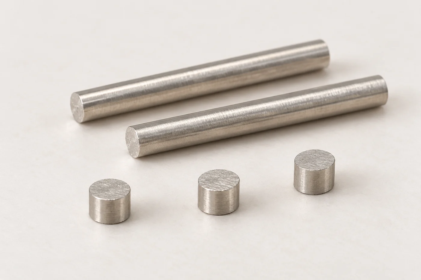
접점 머리의 성능이 좋아도 캐리어와의 접합이 불안정하면 조립품 저항과 온도상승이 커질 수 있습니다. 리벳팅, 저항용접, 브레이징은 접합 원리가 다르며 관리 항목도 다릅니다. 선택한 AgNi·AgCu 등급의 성형·접합 적합성을 실제 부품 구조와 함께 검토해야 합니다.
리벳팅은 축부를 소성변형시켜 기계적으로 고정합니다. 변형량이 부족하면 흔들림이나 회전이 남을 수 있고, 과도하면 캐리어 변형이나 균열, 접점 위치 변화가 생길 수 있습니다. 머리 재질을 바꿀 때는 축부까지 같은 재질인지, 별도 지지재를 가진 복합 리벳인지 먼저 구분합니다.
| 방법 | 관리해야 할 조건 | 확인할 결과 |
|---|---|---|
| 리벳팅 | 돌출 길이·지지·성형량·가압 정렬 | 체결 상태·회전·크랙·접점 높이 |
| 저항용접 | 가압력·전류·시간·전극·표면 | 접합 면적·과열·전극 자국·강도 |
| 브레이징 | 용가재·간극·열 이력·분위기 | 젖음·공극·잔류물·연화 |
| 클래드·복합 구조 | 각 층 재질·두께·계면 | 접합 연속성·층 분리·접촉층 잔여량 |
브레이징의 열은 접점뿐 아니라 프레스 캐리어의 조질과 스프링 성능에도 영향을 줄 수 있습니다. 따라서 접점 경도만 검사하고 조립 후 접촉력은 이전 값으로 가정하면 안 됩니다. 최종 열 공정 뒤의 하중-변위, 접점 높이와 접합부 전압강하를 같은 조립품에서 연결해 확인합니다.
복합 접점은 접촉면의 재료와 지지부의 재료를 각각 선택할 수 있는 구조입니다. 이때 접촉층이 실제 마모와 침식 뒤에도 남아 있어야 하며, 측면 노출이나 접합 계면의 위치가 작동면에 미치는 영향도 보아야 합니다. 단면을 구분하는 3D는 이 재질 경계를 읽기 위한 것으로, 화면의 층 비율을 납품 두께로 해석하지 않습니다.
접합 강도와 통전 건전성은 서로 다른 결과입니다. 강하게 붙어 있어도 전류가 통과하는 유효 면적이 작으면 국부 발열이 생길 수 있습니다. 반대로 처음 저항이 낮아도 진동·열 반복 뒤 고정 상태가 변할 수 있으므로 기계 검사와 전기 검사를 함께 설계해야 합니다.
AgCu = 합금 체계 · Ag/Cu = 이 예제의 층상 구조 표기
이 예제의 Ag/Cu는 Ag 접점층을 Cu 지지부에 접합한 구조 표기입니다. 서로 다른 기능을 맡는 층과 그 사이의 접합 건전성을 함께 검토해야 합니다.
원형 머리와 하나의 동축 축을 가진 접점의 단면 개념입니다. 절개 버튼으로 전체 외형과 닫힌 절단면을 비교할 수 있습니다. 머리·축 비율과 Ag 층 두께는 실제 도면값이 아닙니다. Ag/Cu 구조의 모든 상용 제품이 같은 형상이나 접합 공정을 쓰는 것은 아닙니다. 표기 관행은 공급사마다 다를 수 있으므로 도면과 재료 사양에서 합금 조성, 접점층, 지지 재료와 접합 방법을 별도로 확인합니다.
은계 재료는 산화만으로 표면 상태를 설명할 수 없습니다. 황을 포함한 분위기에서는 은 황화물이 문제될 수 있고, AgCu에서는 구리 관련 산화도 검토해야 합니다. 유기 잔류물과 미세 입자, 포장·보관 환경 역시 실제 접촉 계면을 바꾸므로 광택이 좋다는 이유로 전기적 청정도를 보증할 수 없습니다.
오랫동안 작동하지 않는 저부하 접점에서는 표면막이 제거되지 않은 채 첫 접촉을 맞을 수 있습니다. 반대로 강한 개폐 아크나 미끄럼은 표면을 변화시키면서 마모와 침식도 유발합니다. 처음 작동할 때의 안정성과 지속 작동 뒤의 내구성을 서로 다른 시험 시점으로 나누어야 합니다.
| 관찰 현상 | 가능한 원인 후보 | 추가 확인 |
|---|---|---|
| 표면 변색과 저항 상승 | 황화·산화·유기막 | 노출 이력, 표면 분석, 힘별 저항 |
| 국부 돌기·크레이터 | 전이·아크 체류·융착 분리 | 짝 접점, 극성, 개폐 파형 |
| 접점 가장자리 균열 | 성형 결함·열 이력·기계 하중 | 단면, 조질, 조립 응력 |
| 접합부 주변 변색·발열 | 접합 저항·국부 열 집중 | 구간별 전압강하, 단면, 온도 |
| 반복 작동 후 저항 산포 | 하중 변화·마모편·표면막 | 접촉력, 동적 신호, 오염 분석 |
SEM-EDS는 손상 위치의 원소 분포와 이종 재료 전이를 확인하는 데 유용합니다. 그러나 원소가 검출되었다는 사실만으로 산화물·황화물의 화학 상태까지 확정할 수는 없습니다. 필요한 경우 표면 민감 분석이나 회절 분석을 결합하고, 세정 전 시료를 보존해 원래의 막과 잔류물을 잃지 않도록 합니다.
내변색 후처리도 전기적 평가가 필요합니다. 외관 변화를 억제하는 보호막이 낮은 접촉력에서 계면저항을 높일 수 있기 때문입니다. 후처리 유무를 비교할 때는 외관, 마찰·마모, 초기 저항과 환경 노출 뒤 저항을 함께 기록합니다.
고장 분석용 시료는 닦거나 반복 개폐하기 전에 측정 순서를 정합니다. 세정으로 저항이 내려갔다면 오염 가능성을 뒷받침할 수 있지만, 원래 고장이 무엇이었는지 확인할 증거도 사라질 수 있습니다. 정상품·불량품·미사용품을 같은 위치와 방법으로 비교하는 편이 단일 사진보다 판단력이 높습니다.
접촉저항은 전류를 흘리는 두 선과 전압을 읽는 두 선을 분리하는 4단자 방식으로 측정하는 것이 기본입니다. 전압 검출점 위치에 따라 접점 계면을 중심으로 평가하거나 캐리어와 접합부를 포함할 수 있으며, 검출점 사이의 벌크저항도 측정에 포함됩니다. 시험 도면에 검출점과 도체 구간을 남겨야 시험실과 공급사 결과를 비교할 수 있습니다.
미소 신호 접점의 표면막을 보려면 측정 자체가 막을 파괴하지 않도록 해야 합니다. 계측기 기술자료에서 일반적으로 설명하는 드라이 회로 조건은 개방전압 20 mV 이하, 단락전류 100 mA 이하입니다. 이는 모든 접점에 적용되는 합격 규격이 아니라 비파괴적인 계면 평가를 위한 측정 개념이며, 실제 적용 규격과 제품 조건을 우선합니다.
| 단계 | 측정 내용 | 판정의 초점 |
|---|---|---|
| 초기·보관 후 | 외관, 접촉력, 낮은 에너지의 저항 | 첫 접촉의 안정성과 산포 |
| 정상 통전 | 전압강하, 온도상승, 하중 유지 | 열적으로 안정된 조립품 상태 |
| 반복 개폐 | 바운스, 아크, 융착, 저항 추이 | 실제 부하에서의 고장과 변화율 |
| 환경·기계 노출 후 | 저항, 접합, 층 두께, 형상 | 표면막·마모·체결 상태의 변화 |
| 분해 분석 | 양쪽 접점과 접합부의 단면·표면 | 관찰된 기능 저하와 원인의 연결 |
저항을 낮추기 위해 큰 시험 전류를 먼저 흘리면, 처음 존재했던 표면막이나 미세 접촉점이 바뀔 수 있습니다. 따라서 드라이 회로 평가가 필요하다면 고전류 시험보다 앞에 배치합니다. 열기전력 오차에는 극성 반전이나 오프셋 보상 등을 검토하고, 시료 온도와 측정 대기 시간을 일정하게 유지합니다.
수명 시험에서는 정격 전류 숫자만 남기지 않습니다. 부하 회로, 공급 전압, 투입 피크와 지속시간, 개폐 속도, 접촉력, 바운스, 작동 주기, 주변 온도와 극성을 함께 기록합니다. 합격 기준도 “작동함”보다 개방 실패, 허용 전압강하, 최대 온도상승, 잔여 접점층처럼 기능과 연결되는 항목으로 정합니다.
표본 수와 로트 수가 적은 시험에서 고장이 없었다고 전체 제품의 수명이 증명되는 것은 아닙니다. 개별 시료의 추이와 최악값, 중도 고장과 종료 조건을 남겨야 합니다. 재료를 비교할 때는 시험 순서와 지그·측정 계통의 차이가 특정 재질에만 유리하게 작용하지 않도록 관리합니다.
AgNi와 AgCu 선택은 재료표에서 가장 높은 숫자를 찾는 작업이 아닙니다. 실제 고장이 낮은 신호의 접촉 불안정인지, 투입 융착인지, 반복 아크 침식인지, 미끄럼 마모인지 먼저 정해야 합니다. 같은 부품 안에서도 접점 머리와 캐리어가 만족해야 하는 요구는 다릅니다.
| 주된 사용 조건 | AgNi 검토의 초점 | AgCu 검토의 초점 | 공통 검증 |
|---|---|---|---|
| 반복 개폐 | Ni 분산과 침식·융착 거동 | Cu 함량과 침식·표면막 변화 | 실제 부하 파형과 개방 실패 |
| 미끄럼 접촉 | 등급·상대재·마모편 | 조질·상대 표면·마찰과 마모 | 전압 잡음과 마모 후 형상 |
| 장기 정지·미소 부하 | Ni 함량과 표면 상태 | Cu 관련 산화와 표면 상태 | 보관 후 첫 접촉 저항 |
| 연속 통전 | 벌크·계면·접합 저항 | 벌크·계면·접합 저항 | 실장 상태의 온도상승 |
| 리벳·복합 조립품 | 접점층과 축부의 재질 구분 | 합금층과 Cu 지지부 구분 | 체결·접합·잔여 접점층 |
일반적인 개폐 접점의 후보를 고를 때 AgNi10·15·20은 검토 가치가 있지만, 숫자가 큰 등급부터 고르는 방식은 적절하지 않습니다. 사용 가능한 접촉력, 구동력과 접점 크기가 제한되어 있다면 저항 상승이 먼저 문제가 될 수 있습니다. 후보 재질을 두세 가지로 좁힌 뒤 같은 작동 조건에서 고장 모드를 비교합니다.
AgCu가 기계적 마모에서 유리한 결과를 보였더라도 그것만으로 개폐 접점의 아크 수명을 보증할 수 없습니다. 무통전 마찰시험과 통전 미끄럼시험은 열·전기적 영향이 다르고, 정지 접촉과 회전 접촉은 표면이 갱신되는 방식이 다릅니다. 실제 상대재와 표면처리까지 맞춘 시험이 필요합니다.
미소 신호와 장기 보관이 핵심이라면 AgNi와 AgCu만으로 선택지를 제한할 이유는 없습니다. 필요한 경우 적절한 귀금속 표면처리나 다른 접점계를 검토하되, 그 층이 개폐 아크나 마모 뒤에도 요구 기능을 유지하는지 확인해야 합니다. 얇은 표면층을 추가한 재료는 무처리 벌크 재료와 별도의 사양입니다.
소재 변경의 성공 기준은 새 재질이 특정 물성 하나에서 앞서는 것이 아니라, 완성품이 필요한 기능을 반복해서 유지하는 것입니다. 후보 재료가 달라지면 성형·접합·세정 조건도 다시 검토하고, 그 변경을 포함한 상태에서 저항·발열·내구를 확인합니다. 한 조건에서의 개선이 다른 조건의 여유를 줄이지 않는지까지 확인해야 합니다.
도면에 “은접점” 또는 “AgNi”만 적으면 성분과 조질, 구조가 충분히 정의되지 않습니다. 접점 머리와 지지부를 구분하고, 필요한 경도와 검사 시점, 접합 방법과 기능 기준을 함께 지정해야 합니다. 재질 성적서는 이 사양을 확인하는 자료이며 완성품의 모든 접촉 성능을 대신하지 않습니다.
| 도면·발주 항목 | 구체적으로 지정할 내용 |
|---|---|
| 재질 | AgNi 또는 AgCu 세부 등급, 성분 범위, 적용 재료 규격 |
| 구조 | 단일재·복합재·도금 구분, 각 층/축부/캐리어 재질 |
| 상태 | 공급 조질과 최종 열 이력 뒤 경도, 시험 하중·위치 |
| 기하 | 접촉면 형상·높이·편심, 층 두께와 허용 결함 |
| 접합 | 리벳·용접·브레이징 조건과 확인 항목 |
| 기능 | 접촉력, 저항 측정점·전류·전압, 온도상승과 내구 조건 |
| 추적·변경 | 원재료 로트, 제조사·공정·표면처리 변경 승인 범위 |
화학 분석과 표면 분석도 목적을 구분합니다. 표면을 보는 XRF 결과만으로 얇은 층 아래까지 포함한 전체 조성을 확정하기 어려운 구조가 있습니다. 층상 구조에서는 단면 관찰과 깊이·위치가 정의된 분석을 사용하고, 조성과 조직을 혼동하지 않도록 검사 방법을 선택합니다.
먼저 기존품의 고장 모드와 사용 조건을 문서화하고 변경 목적을 정합니다. 다음으로 후보 재질의 성분·조직·조질을 확인해 성형과 접합 조건을 설정합니다. 이후 최종 조립품으로 초기 성능, 환경 노출과 반복 작동을 평가하고, 기존품과 같은 판정 기준으로 비교합니다.
검사 기록에는 좋은 결과뿐 아니라 분포와 실패 형태를 남깁니다. 초기 저항이 낮아도 특정 로트에서 균열이 늘거나 수명 뒤 접촉력이 감소하면 그대로 승인하기 어렵습니다. 공급사·분말 또는 주조 경로·열처리·표면처리 변경 중 무엇이 재시험을 요구하는지도 함께 정합니다.
아이디메탈에 전기접점 제작을 문의할 때는 접점과 캐리어 도면, 현재 사용 재질, 상대 접점, 부하 회로, 접촉력과 요구 수명 조건을 함께 전달해 주세요. 실측 불량이 있다면 저항·온도·파형과 손상 사진을 연결하면 재질과 제조 공정을 더 구체적으로 검토할 수 있습니다. 조성만 바꾸는 접근보다 접점 구조와 사용 조건을 함께 정의하는 접근이 정확한 비교를 만듭니다.
AgNi의 핵심은 니켈 분산 조직을 활용하는 방식이고, AgCu의 핵심은 구리 함량과 가공·열 이력이 만드는 성질입니다. 두 재료의 우열은 전도율이나 경도 하나로 정해지지 않습니다. 실제 접촉력·표면·접합·부하 조건에서 저항 안정성과 마모·침식·융착을 함께 확인하는 것이 전기접점 재질 선정의 기준입니다.
AgNi and AgCu electrical contacts can look similar while differing in internal structure and surface behavior. The dispersed structure of silver–nickel, the alloy condition of silver–copper, working and thermal history affect resistance, wear, arc erosion and welding in different ways.
Selection starts with the actual contact duty, rather than a ranking of silver content or hardness. Continuous current carrying, repeated interruption and sliding against a counterface demand different properties. Distinguish detailed grades and supplied conditions, then compare the finished assembly with its contact force, surfaces and joints.
Material and structure
Distinguish dispersed Ni in AgNi from the alloy condition of AgCu.
Contact and switching
Connect conductivity, films, force and arc damage.
Manufacture and verification
Translate selection into forming, joining, tests and drawings.
A switching contact must carry current while closed and interrupt it as it opens. These two duties do not demand identical material properties. Even silver, which is favorable for low electrical resistance, can deform, wear, transfer material and weld during repeated impact, sliding and arcing.
AgNi is a family that uses nickel dispersed in silver to modify contact durability, whereas AgCu uses copper alloying to adjust the mechanical and electrical behavior of silver. Suitability depends on the actual duty of the contact, not simply its alloy name. Start by distinguishing current carrying, switching and sliding contact.
| Aspect | AgNi | AgCu |
|---|---|---|
| Microstructural basis | Silver matrix with a separate nickel phase | Ag-rich and Cu-rich phases; solution and precipitation depend on condition |
| Material variables | Nickel content, distribution, orientation and density | Copper content, temper, thermal history and surface oxidation |
| Contact verification | Resistance, erosion, welding and material transfer | Resistance, wear, oxidation and material transfer |
| Not established by the name | Allowable current, life or actual contact force | Allowable current, life or actual contact force |
The silver-based contact head and a copper-based carrier have different functions. The head provides the mating surface; the carrier supplies a current path and mechanical support or spring action. Calling the entire assembly an AgCu alloy merely because its carrier is copper confuses material with construction.
Define the head composition, solid or composite construction, opposing material and contact geometry together. A test using a high force on AgNi and a low force on AgCu does not isolate the material effect. Either change the material under matched finished-part conditions or document every design adjustment made for the alternative material.
The photographs in this article are generated illustrations of contact geometry and assembly relationships. They do not document the composition, dimensions or inspection results of delivered products. The interactive sections explain material structure and current paths; they are not micrographs or life predictions for a particular product.
Silver and nickel have negligible mutual solid solubility and limited mutual solubility in the liquid state. Conventional higher-nickel AgNi contact materials therefore disperse a nickel phase within silver rather than forming one uniform phase. Silver provides current and heat paths, while the distribution and shape of nickel influence surface deformation and erosion.
The numbers in AgNi10, AgNi15 and AgNi20 normally identify nominal nickel mass percentages. They are not directly equal to the area fraction seen in a micrograph or the volume fraction. Verify both the nominal designation and permitted composition range; for a composite rivet, specify the contact layer and backing separately.
| Family | Structure and manufacture | Selection caution |
|---|---|---|
| AgNi0.15 | A small nickel addition restrains silver grain growth | Do not scale its behavior as a diluted version of AgNi10. |
| AgNi10, 15 and 20 | Dispersed nickel in silver, commonly made by powder metallurgy | Check distribution, density and temper as well as content. |
| AgNi30 and 40 | A higher nickel fraction in the composite | Review resistance, formability and required contact force together. |
After powder blending, compaction and sintering, extrusion and drawing can elongate nickel particles along the working direction. The same stock may show fibers in a longitudinal section and separate particles in a transverse section. Record the observation direction before judging dispersion quality from different sections.
Increasing nickel changes more than composition: it also changes the continuous silver conduction paths, hardness and deformation capacity. Higher-nickel grades may help in particular switching duties, but the contact force and operating mechanism must support their use. More nickel does not automatically extend life under every load.
Use the structural view to understand the relationship between the silver matrix and dispersed phase. Particle sizes and spacing shown on the screen are not manufacturing specifications. Assess real material uniformity by linking metallography at defined locations with composition, density and property measurements.
Copper can dissolve in silver, but its solid solubility is limited. Ag-rich and Cu-rich phases can coexist depending on temperature and composition, and cooling rate and subsequent heat treatment change their size and distribution. AgCu should therefore not be described as copper permanently dissolved uniformly throughout all the silver.
AgCu3 and AgCu10 belong to the same silver–copper system but differ in copper content and supplied condition. Copper is used to strengthen silver, and cold working also changes hardness. Even where a composition can show solution-treatment, cooling and aging effects, confirm separately whether the delivered product is actually specified as age hardened.
| Designation or construction | Meaning | Drawing information |
|---|---|---|
| AgCu10 | Normally a silver–copper alloy with about 10 mass% Cu | Composition limits and supplied temper |
| Layered Ag/Cu | A composite joining a silver layer to copper | Each layer material, thickness and interface quality |
| AgNi/Cu composite contact | An AgNi contact layer with a Cu backing | Contact composition, remaining thickness and bond condition |
| Silver-plated copper | A deposited silver coating on a copper substrate | Plating thickness, porosity, adhesion and wear conditions |
Slash notation varies among suppliers and publications. For example, Ag/Ni can denote a nickel-dispersed composite rather than a layered construction. Establish alloy, dispersed composite, clad or plated construction from the material description and section drawing, not punctuation alone.
The NIST Ag–Cu equilibrium calculation places the eutectic reaction at about 779°C and a liquid composition of about 28.4 mass% Cu. This does not mean that every part of AgCu3 or AgCu10 melts simultaneously at that temperature. Use the composition-specific solidus, liquidus and actual thermal history; the eutectic temperature is not an allowable contact service temperature.
One supplier’s AgCu3 sheet explicitly lists the material as not age hardenable. It is therefore inappropriate to claim that every AgCu grade is strengthened by aging. In manufacturing, it is more useful to check how much cold-worked hardness survives brazing or annealing, using the finished contact’s hardness and deformation.
As copper content rises, evaluate mechanical benefits alongside the burden of surface oxidation. Copper-rich regions influence strength and wear, while oxides at the contact surface alter the current-carrying interface. An AgCu sliding contact whose surface is continually renewed requires a different assessment from a lightly loaded contact that remains inactive for a long time.
AgNi dispersed phases ≠ AgCu alloy microstructure
This is a schematic of Ni dispersed in an Ag matrix. Elongated marks illustrate possible alignment after processes such as extrusion; they do not represent the particle shape or microstructure of every product.
Colors, domain sizes and counts distinguish phases only. This is not microscopy, measured grain size, phase fraction or a reconstruction of a manufacturing microstructure. It does not imply that AgCu is mixed in the same way as Ni particles. Alloy names alone do not calculate contact resistance, arc-erosion resistance or life. Composition, manufacturing history and actual contact tests must be considered together.
Conductivity data are a starting point for understanding materials, not a table of contact life. The following examples use published ranges from one supplier, Heraeus. They are not results from a comparison with one matched product form and temper, and the endpoints of the conductivity and hardness ranges do not necessarily describe the same specimen condition.
| Published grade | Conductivity, %IACS | Vickers hardness, HV | Nature of data |
|---|---|---|---|
| AgCu3 / Hera 343 | 90.53–95.56 | 45–95 | Published property range |
| AgCu10 / Hera 342 | 81.9–86 | 65–120 | Published property range |
| AgNi10 / Hera 367 | 81.9–86 | 50–90 | Temper-dependent range |
| AgNi20 / Hera 365 | 74.78–78.18 | 60–110 | Published property range |
IACS is a reference scale for electrical conductivity. At 20°C, 100% IACS corresponds to approximately 58 MS/m; %IACS is not silver content. The individual conductivity entries do not separately state a measurement temperature, so they must not be extrapolated to an arbitrary elevated-temperature condition. Confirm measurement temperature, method and guaranteed limits when purchasing.
AgNi10 and AgCu10 have identical conductivity ranges in this table. It therefore does not support a universal ranking in which nickel-containing material always conducts less well than AgCu. Another manufacturer may publish different values for the same nominal grade. Combining extrema from different suppliers into a single representative value conceals processing, structure and condition differences.
Hardness also depends on test load and measurement location. Do not directly equate results at different loads, such as HV1 and HV10, or results from a thin contact layer and a sufficiently thick sample. Establish conditions that limit interference from the backing, edges and neighboring indentations.
For example, one AgCu20 sheet distinguishes 80–120 HV in the annealed condition from 130–190 HV after work hardening. The alloy name can remain unchanged while its deformation history changes the properties. Specify the required hardness after final heat treatment and joining, and verify its effects on both contact resistance and cracking.
Two apparently mating contacts do not touch metal-to-metal across their entire nominal area. Only some microscopic asperities form conducting spots, and current converges into those small regions. The resulting constriction resistance and surface-film effects must be distinguished from resistance within the bulk material.
Contact force changes the real contact area. A harder material may resist wear yet give higher interface resistance if it forms insufficient contact area under the same load. Increasing force also changes actuator demand, spring stress, impact and wear, so material selection cannot be separated from mechanism design.
| Resistance location | Key variables | How to distinguish it |
|---|---|---|
| Within the material | Conductivity, length, section and temperature | A defined specimen or conductor-segment measurement |
| Mating contact interface | Real area, force and films | Four-terminal measurement under controlled contact force |
| Contact-to-carrier joint | Bond area, oxide, voids and fastening | Voltage sensing on opposite sides of the joint |
| Complete assembly | Combined resistances and heat paths | Voltage drop and temperature rise in the installed configuration |
As an illustrative calculation, a fixed contact resistance of 1 mΩ dissipates 0.1 W at 10 A and 0.9 W at 30 A. Tripling current increases dissipation ninefold at the same resistance. This estimates electrical heating power, not temperature rise, which also depends on heat paths through the carrier, terminals and surrounding air.
When comparing AgNi and AgCu, the resistance distribution after repeated operation matters more than one low initial reading. A low average can conceal occasional large voltage drops that interrupt signals. For power-carrying parts, record stabilized temperature and resistance together to distinguish a material issue from loss of force or a joint problem.
The resistance model separates current paths and interface locations. Its simplified contact spots and controls do not reproduce actual roughness, oxide-film thickness or a particular alloy grade. Use measurements at matched contact force and surface condition for a real material comparison.
Rb = ρL/A · R = Rb + Rc · V = IR · P = I²R
The equivalent bulk path has total length L=20 mm and area A=4 mm². One contact-interface resistance Rc is added in series; additional joint resistances are excluded. Resistivity and interface resistance are independent hypothetical inputs, not representative AgNi/AgCu values or test results. The 3D identifies the interface; it does not solve resistance from the rivet geometry. The blue line locates the interface and is not an insulating film or a gap. Resistivity is assumed constant. Heat transfer, temperature rise, contact pressure, microscopic constriction resistance, oxide-film evolution, switching arcs and life are not calculated. At 0 A loss is zero; the colored bar below shows resistance shares.
If current does not cease immediately as contacts separate, an arc can form across the small gap. Repeated local melting, evaporation and movement of molten metal create craters and protrusions. Closing bounce can also produce repeated short interruptions and recontacts, causing localized damage.
The separate nickel phase in AgNi changes erosion and transfer behavior relative to silver alone. This does not make AgNi immune to arc-induced melting. Dispersion, porosity, contact size, opposing material and arc residence location all affect damage, so composition and structure must be considered together.
AgNi is considered not simply for the highest conductivity, but to combine silver conduction with the erosion and transfer control provided by a dispersed phase. Supplier literature describes improved erosion resistance relative to silver and silver alloys in applicable switching conditions. This does not establish superiority over every AgCu grade in every circuit; verify the balance between low resistance and welding control under the actual load.
| Mechanism | Observable result | Operating conditions to record |
|---|---|---|
| Arc erosion | Mass change, depth, volume loss and roughness | Voltage/current waveforms and arc duration |
| Welding | Failure to open, separation force and frequency | Making current, bounce and opening mechanism |
| Material transfer | Protrusion on one side and crater on the other | DC polarity, load type and switching speed |
| Film accumulation | Resistance distribution and surface chemistry | Atmosphere, idle time and contact force |
Copper additions also change strength, erosion and transfer relative to pure silver. However, oxidation associated with increased copper content can adversely affect resistance after repeated switching. Do not reduce AgNi–AgCu comparison to one “arc resistance” score; separate erosion, welding and resistance growth according to the actual failure criteria.
AC current zeros, DC polarity, stored energy in inductive loads and inrush into capacitive loads are distinct conditions. A supplier’s application-current example must not be copied as a universal material rating. Even at the same stated current, source impedance and protective circuitry can change the waveform imposed on the contacts.
Analyze material transfer as a mating pair. Mass loss from one contact alone cannot distinguish evaporation from transfer to the opposing contact. Record both masses, surface profiles, the remaining open gap and changes in mating position to identify the path toward failure.
Academic results must likewise be read within their test conditions. A 2024 study of additions to AgNi tested experimental specimens 3.2 mm in diameter and 2.5 mm high for 100,000 operations under a 24 V DC, 15 A resistive load in air at 0.86 N contact force. It investigated specific powder-metallurgical specimens and additives; it was neither a direct commercial AgNi10–AgCu10 comparison nor a product-life guarantee. Match composition, processing, geometry and circuit conditions before applying such findings.
A representative AgNi route comprises silver and nickel powder preparation, blending, compaction, sintering, densification and working. Particle size, agglomeration and mixing uniformity establish the starting nickel distribution. Residual pores or large agglomerates can affect forming and contact-surface damage, so chemistry alone does not establish manufacturing quality.
A typical AgCu route produces semifinished material by alloy melting and casting followed by rolling or drawing. Cast structure and segregation are controlled, and working and annealing are combined to obtain the required dimensions and hardness. Results for a research powder-processed Ag–Cu composite cannot automatically be applied to conventional silver-rich AgCu wire.
| Stage | Material condition that matters | Finished-part check |
|---|---|---|
| Incoming wire or strip | Composition, temper, diameter/thickness and surface | Lot traceability and certificate matching |
| Cutting and cold forming | Hardness, ductility and working direction | Head eccentricity, cracking and laps |
| Annealing or heat exposure | Temperature, time and atmosphere | Hardness change, oxidation and distortion |
| Cleaning and handling | Residues, particles and surface protection | Contact contamination and recontamination control |
For head forming, consider material flow and die contact. An excessively hard condition may not accommodate the required strain; an excessively soft condition can create different problems in shape retention and assembly. Inspect cracking, laps, surface defects and hardness alongside final dimensions.
Changing powder, sintering or extrusion conditions can change the structure and density of the same AgNi grade. Changing cold reduction and thermal history can alter hardness and ductility within the same AgCu grade. An unchanged chemistry designation is therefore insufficient to approve an untested supplier or manufacturing-route substitution.
In process development, work back from the required finished behavior to the incoming stock condition. Define final force, geometry and contact-layer thickness, then choose stock that can retain those requirements through forming and joining. Tracking the change from incoming to finished hardness helps locate the process stage where defects begin.
A capable contact head cannot compensate for an unstable carrier joint, which can increase assembly resistance and temperature rise. Riveting, resistance welding and brazing have different joining mechanisms and control variables. Review the formability and joining suitability of the selected AgNi or AgCu grade in the actual part construction.
Riveting plastically deforms the shank to produce mechanical retention. Insufficient forming can leave looseness or rotation, while excessive forming can distort or crack the carrier and shift the contact position. Before changing head material, establish whether the shank is the same material or belongs to a composite rivet with separate backing.
| Method | Conditions to control | Results to verify |
|---|---|---|
| Riveting | Protrusion, support, forming amount and alignment | Retention, rotation, cracks and contact height |
| Resistance welding | Force, current, time, electrodes and surfaces | Bond area, overheating, electrode marks and strength |
| Brazing | Filler, gap, thermal history and atmosphere | Wetting, voids, residues and softening |
| Clad or composite construction | Layer materials, thicknesses and interface | Bond continuity, separation and remaining contact material |
Brazing heat can affect the temper and spring behavior of a stamped carrier as well as the contact. Checking head hardness while assuming that the assembled force remains unchanged is inadequate. Link force–displacement, contact height and joint voltage drop after the final thermal process on the same assembly.
Composite contacts allow the mating-surface material and backing material to be selected separately. The contact layer must remain adequate after the required wear and erosion, and side exposure or interface location may also affect the working surface. The cutaway view explains these material boundaries; its layer proportions are not delivery thicknesses.
Joint strength and electrical integrity are different outcomes. A mechanically strong joint can still heat locally if the effective current path is small. Conversely, low initial resistance does not guarantee stable retention after vibration or thermal cycling, so mechanical and electrical checks must be designed together.
AgCu = alloy system · Ag/Cu = the layered notation used here
Here Ag/Cu denotes an Ag contact layer bonded to a Cu backing. The layers perform different functions, and the integrity of the bond between them also requires evaluation.
This section illustrates a round head and one coaxial shank. Toggle the quarter-cut view to compare the complete exterior and closed section faces. Head/shank proportions and Ag-layer thickness are not drawing dimensions. Commercial Ag/Cu contacts do not all share this shape or bonding process. Notation varies between suppliers: identify alloy composition, contact layer, backing material and joining method separately in the drawing and material specification.
Oxidation alone does not describe the surface condition of silver-based materials. Silver sulfide can matter in sulfur-containing atmospheres, while copper-related oxidation must also be considered for AgCu. Organic residues, fine particles, packaging and storage also alter the interface; a bright appearance does not guarantee electrical cleanliness.
A low-load contact left idle for a long time may first close with its surface film still present. Arcing or sliding can alter that film, but also introduces wear and erosion. Treat first-operation reliability and durability after sustained operation as separate test points.
| Observation | Possible causes | Additional evidence |
|---|---|---|
| Discoloration and resistance rise | Sulfide, oxide or organic film | Exposure history, surface analysis and resistance versus force |
| Localized protrusion or crater | Transfer, arc residence or weld separation | Mating partner, polarity and switching waveforms |
| Crack near a contact edge | Forming defect, heat exposure or mechanical load | Section, temper and assembly stress |
| Heat or discoloration near a joint | Joint resistance or localized heating | Segment voltage drop, cross-section and temperature |
| Resistance scatter after cycling | Force change, wear debris or films | Contact force, dynamic signals and contamination analysis |
SEM-EDS is useful for elemental distribution at damaged regions and for identifying transferred material. Detecting an element does not, by itself, establish the chemical state of an oxide or sulfide. Where needed, combine surface-sensitive or diffraction methods, and preserve uncleaned samples so that the original films and residues are not lost.
Anti-tarnish treatments also require electrical evaluation. A film that preserves appearance can increase interface resistance at low contact force. Compare treated and untreated surfaces using appearance, friction or wear, initial resistance and resistance after environmental exposure.
Set the measurement sequence before wiping or repeatedly operating a failed sample. A resistance drop after cleaning can support a contamination hypothesis, but cleaning can also remove evidence of the original failure. Comparing good, failed and unused parts at matched locations is more informative than judging one photograph.
A four-terminal arrangement separates the two current leads from the two voltage-sensing leads for low-resistance measurement. Sense-point placement can focus the evaluation on the mating region or include carriers and joints; bulk resistance between the sense points is still included. Document the sense points and conductor segments before comparing laboratory and supplier results.
To examine films on a low-level contact, the measurement must not break down the film itself. Instrumentation guidance commonly describes dry-circuit conditions as no more than 20 mV open-circuit voltage and 100 mA short-circuit current. These are measurement conditions intended to avoid altering the interface, not universal contact acceptance limits; use the applicable product specification.
| Stage | Measurements | Assessment focus |
|---|---|---|
| Initial and after storage | Appearance, contact force and low-energy resistance | First-contact reliability and scatter |
| Normal current carrying | Voltage drop, temperature rise and retained force | Thermally stabilized assembly behavior |
| Repeated switching | Bounce, arc, welding and resistance history | Failure and change under the actual load |
| After environmental or mechanical exposure | Resistance, joints, layer thickness and geometry | Changes in films, wear and fastening |
| Destructive analysis | Both contact surfaces and joint sections | Linking functional degradation to its cause |
Applying a large test current first can change the original films or microscopic contact spots. Place dry-circuit evaluation before higher-current testing when preservation of that state matters. Consider current reversal or offset compensation for thermoelectric errors, and control specimen temperature and settling time.
An endurance record requires more than a rated-current number. Record the load circuit, supply voltage, inrush peak and duration, operating speed, force, bounce, duty cycle, ambient temperature and polarity. Define acceptance in functional terms such as failure to open, allowable voltage drop, maximum temperature rise and remaining contact layer, rather than merely “still operates.”
No failures in a small sample or a single lot do not prove the life of the entire product population. Retain individual histories, worst cases, early failures and stopping conditions. Control test order, fixtures and measurement-system differences so that they do not systematically favor one material.
Selecting AgNi or AgCu is not a search for the largest number in a datasheet. First identify whether the limiting failure is low-level contact instability, making-current welding, repeated arc erosion or sliding wear. Even within one part, the head and carrier have different requirements.
| Primary duty | AgNi assessment | AgCu assessment | Common verification |
|---|---|---|---|
| Repeated switching | Ni dispersion, erosion and welding | Cu content, erosion and film evolution | Actual load waveform and failure to open |
| Sliding contact | Grade, opposing material and debris | Temper, counterface, friction and wear | Voltage noise and worn geometry |
| Long idle periods and low-level loads | Ni content and surface condition | Copper-related oxidation and surface condition | First-contact resistance after storage |
| Continuous current carrying | Bulk, interface and joint resistance | Bulk, interface and joint resistance | Temperature rise in the installed state |
| Riveted or composite assembly | Separate head and shank materials | Separate alloy layer and Cu backing | Retention, bond and remaining contact layer |
AgNi10, AgNi15 and AgNi20 are useful candidates for many switching-contact reviews, but starting with the highest nickel number is not a sound selection rule. Where available force, actuator capacity or contact size is limited, resistance rise may become the limiting issue. Narrow the candidates and compare their failure modes under matched operating conditions.
A favorable AgCu mechanical-wear result does not guarantee arc life in a switching contact. Unpowered friction tests and current-carrying sliding tests differ in electrical and thermal effects, while stationary and rotating contacts renew their surfaces differently. Test the actual opposing material and finish as well.
For low-level signals and long storage, there is no reason to restrict the choice to AgNi and AgCu alone. Appropriate precious-metal finishes or other contact systems may be considered, but their function must survive the required arcing and wear. A material with an added thin surface layer is a separate specification from the untreated bulk material.
A successful material change is one that repeatedly preserves the required finished-part function, not simply one that improves a single property. Revisit forming, joining and cleaning when the candidate changes, then assess resistance, heating and endurance in that final condition. Check whether an improvement in one duty reduces margin in another.
“Silver contact” or “AgNi” alone does not sufficiently define composition, temper and construction. Separate the head from its backing, and specify hardness, inspection stage, joining method and functional criteria. A material certificate supports that specification; it does not replace all finished-contact performance verification.
| Drawing or purchase item | What to specify |
|---|---|
| Material | Detailed AgNi or AgCu grade, composition limits and material specification |
| Construction | Solid, composite or plated; each layer, shank and carrier material |
| Condition | Supplied temper and hardness after final heat exposure; test load and location |
| Geometry | Contact profile, height, eccentricity, layer thickness and permissible defects |
| Joining | Riveting, welding or brazing requirements and verification |
| Function | Force, resistance sense points/current/voltage, heating and endurance conditions |
| Traceability and change | Stock lot and approval scope for supplier, process or finish changes |
Distinguish the purposes of chemical and surface analysis. In some layered constructions, a surface-sensitive XRF result cannot establish the overall composition beneath a thin layer. Use cross-sections and analyses with defined depth and location, and choose methods that distinguish chemistry from microstructure.
First document the existing failure mode and service conditions, then define the purpose of the change. Establish candidate composition, structure and temper before setting forming and joining conditions. Evaluate the final assembly for initial behavior, environmental exposure and repeated operation against the same acceptance criteria as the existing part.
Keep distributions and failure modes as well as favorable results. Low initial resistance does not justify approval if certain lots develop more cracks or lose contact force after endurance. Define which changes in supplier, powder or casting route, heat treatment or finish require requalification.
For an electrical-contact manufacturing inquiry to ID METAL, provide the head and carrier drawings, current material, mating contact, load circuit, contact force and required endurance conditions. If failures have been measured, connect resistance, temperature and waveform data with damage photographs to support a more specific material and process review. Defining construction and duty together provides a sounder comparison than changing chemistry alone.
The central feature of AgNi is its dispersed nickel structure; for AgCu it is the behavior produced by copper content, working and thermal history. Neither conductivity nor hardness alone determines the better material. Electrical-contact selection requires stable resistance, wear, erosion and welding behavior to be assessed under the actual force, surface, joining and load conditions.
AgNi와 AgCu 전기접점은 미세조직, 첨가 원소와 공급 상태를 구분해 비교해야 합니다. 니켈 분산과 은-구리 합금의 차이를 바탕으로 전도율·경도·표면막·접촉저항·침식·융착을 해석하고, 성형과 접합 뒤 실제 접촉력·부하·환경 조건에서 검증하는 것이 재질 선정의 기준입니다.
아닙니다. AgNi는 니켈 분산 조직의 특성을, AgCu는 구리 함량과 가공·열 이력이 만드는 성질을 활용합니다. 실제 접촉력, 상대 재질, 표면 상태와 개폐·미끄럼 조건에서 저항·마모·침식·융착을 비교해야 합니다.
직접 대체하면 안 됩니다. AgNi0.15는 소량의 니켈로 결정립 성장을 억제하는 미립은이며, AgNi10은 통상 분말야금으로 제조하는 니켈 분산 접점재입니다. 조성·조직·공급 상태와 완성품 시험을 확인해야 합니다.
다릅니다. AgCu10은 은-구리 합금의 조성을 나타내고, 은층과 동층이 붙은 구조는 층별 재질·두께·계면으로 정의합니다. 슬래시 표기는 관행이 다르므로 단면도와 공급사 재료 설명으로 확인합니다.
재료 내부 저항에는 유리할 수 있지만 계면저항은 실제 접촉 면적, 접촉력, 경도와 표면막의 영향을 받습니다. 캐리어와 접합부도 전체 측정값에 포함될 수 있으므로 전압 검출점을 명확히 해야 합니다.
아닙니다. 조성과 열 이력에 따라 고용·석출 거동이 달라지고 공급사 AgCu3 자료에는 시효경화 불가로 표시된 사례도 있습니다. 실제 납품 조질과 냉간 가공량, 최종 열 이력 뒤의 경도를 확인해야 합니다.
안 됩니다. 접점 크기와 접촉력, AC/DC, 부하 종류, 투입 전류, 개폐 속도와 보호회로가 다르면 같은 전류에서도 손상이 달라집니다. 정격과 수명은 실제 제품 구조와 적용 시험 조건으로 정합니다.
표면막을 바꾸지 않은 상태를 평가하려면 고전류 시험보다 먼저 측정합니다. 일반적인 계측 지침은 개방전압 20 mV 이하와 단락전류 100 mA 이하를 설명하지만, 최종 조건은 적용 규격과 제품의 측정 목적에 맞춰 정합니다.
접점·캐리어 도면과 재질, 단일재·복합재 구분, 상대 접점, 접촉력, 부하 회로와 파형, 온도·환경·요구 수명을 준비합니다. 불량이 있다면 저항·온도 측정과 손상 위치를 연결한 자료가 도움이 됩니다.
접점 머리는 접촉면의 전기·마모 기능을, 캐리어는 지지·탄성·전류 경로를 담당합니다. 두 재료의 사양과 최종 접합 상태를 각각 정의해야 합니다.
냉간 가공으로 얻은 경도는 성형과 열 노출 뒤 달라질 수 있습니다. 입고 성적서와 최종 부품의 경도·형상·접촉력을 연결해 기록합니다.
재질만 비교하려면 형상·상대재·하중·부하·측정 조건을 맞춥니다. 재질에 맞춰 기구나 공정을 바꿨다면 변경된 시스템 전체를 검증 대상으로 삼습니다.
제품과 제작 범위는 전기접점 사업분야와 정밀 프레스 사업분야에서 확인할 수 있습니다. 접점과 탄성 캐리어의 관계는 리벳 접점 조립품, 축부 성형과 체결은 튜블라 접점 리벳팅의 설명과 연결됩니다.
캐리어 소재를 함께 검토할 때는 프레스 재료별 특성을 참고하고, 접점·캐리어 도면과 사용 조건은 제품문의·개발의뢰로 전달해 주세요.