반세기의 표준 소재 AgPd30 PD100 전기 접점
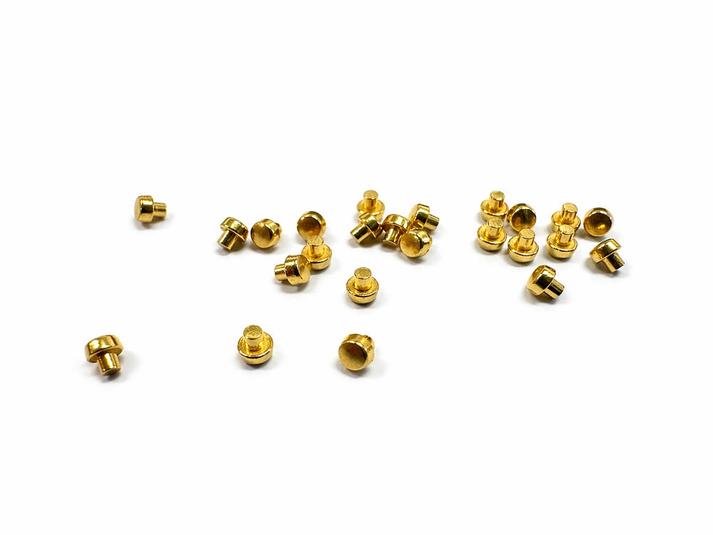
AgPd30 (PD100) 전기접점 - 아이디메탈 ID METAL
AgPd30 (PD100) 전기 접점 소재의 개요
AgPd30은 은(Ag) 70wt%와 팔라듐(Pd) 30wt%를 기본 조성으로 하는 귀금속 합금 접점 소재로서, 통신·자동차·산업용 릴레이와 정밀 스위치의 중간 부하 영역에서 수십 년간 사실상의 표준 재료로 자리 잡고 있습니다. 업계에서는 PD100이라는 상용 코드로 널리 통용되며, Heraeus Precious Metals(구 DODUCO)와 Johnson Matthey, Tanaka Kikinzoku, Umicore 같은 주요 귀금속 제조사가 거의 동일한 사양으로 공급하고 있습니다. 이 소재는 60V/2A 이상의 중간 부하 DC·AC 환경에서 요구되는 전도성, 내아크성, 내황화성, 내마모성이라는 네 가지 조건을 단일 합금으로 동시에 충족시키는 대표적인 사례이며, 같은 계열의 AgPd10, AgPd20, AgPd50 등이 존재하지만 성능과 비용의 균형이 가장 잘 잡힌 지점이 바로 Pd 30wt% 조성이라는 점에서 오늘날까지도 대체되기 어려운 위치를 지키고 있습니다.
AgPd30이 단순한 합금이 아니라 “접점 시스템 재료”로 분류되는 이유는, 실제 사용 조건에서 일어나는 현상이 재료 하나의 물성으로 설명되지 않기 때문입니다. 접촉 계면에서는 μm 단위의 국부 용융과 재응고, 산화와 환원, 원자 확산, 기계적 마모가 동시에 발생하며, 아크 방전 시에는 수천 K에 이르는 플라즈마가 수 ms 단위로 접점 표면을 두들기게 됩니다. 이 극단적 환경에서 장기 신뢰성을 보장하려면 재료의 화학 조성뿐 아니라 결정립 구조, 표면 조도, 산화막 두께, 베이스 금속과의 접합 구조까지 정밀하게 설계되어야 하며, AgPd30은 이 모든 설계 변수를 제어하기 위해 축적된 야금학적 지식의 집약체라 할 수 있습니다.
PD100 명칭의 유래와 개발 배경
PD100이라는 명칭은 1970년대 중반 금(Au) 가격 급등이라는 외부적 충격에서 탄생한 산업적 해법입니다. 1971년 브레튼우즈 체제 붕괴 이후 금 가격은 온스당 35달러 수준에서 1980년에는 850달러까지 폭등했으며, 당시 전 세계 통신 장비와 자동차 전장 시스템의 접점으로 주력 사용되던 22K 금합금 및 Au-Ag-Cu 3원 합금은 비용 구조상 더 이상 유지가 어려웠습니다. 이에 독일의 DODUCO(현 Heraeus), 영국의 Johnson Matthey, 일본의 Tanaka Kikinzoku가 동시다발적으로 Ag-Pd 이원계 합금의 황화 거동과 아크 침식 거동을 체계적으로 연구했고, 그 결과 Pd 함량이 약 30wt% 부근에서 황화 반응 속도가 순수 은 대비 약 1/5 수준으로 급격히 감소하는 임계점이 존재한다는 사실이 확인되었습니다.
PD100이라는 코드는 DODUCO의 내부 상품 분류 체계에서 파생된 것으로, Pd 계열 제품군에서 최초로 대량 상용화된 주력 등급이라는 의미를 갖습니다. 순수 팔라듐을 지칭하는 Pd1000과 구분되며, 순수 Pd는 우수한 내식성에도 불구하고 유기 가스 분위기에서 중합체를 촉매 형성하는 이른바 프릭셔널 폴리머(frictional polymer) 문제 때문에 접점 재료로는 부적합하다는 한계가 알려져 있었습니다. AgPd30은 은 70%의 희석 효과로 이 촉매 활성을 일정 수준 억제하면서도 팔라듐의 내황화성을 상속받는 절묘한 조성이며, 이후 Bell Laboratories, Siemens Research, NTT 연구소 등이 발표한 수명 시험 데이터에서 Au-Ag-Cu 삼원 합금의 약 90% 수준 성능을 40~60% 비용으로 구현한다는 결론이 누적되며 산업 표준으로 정착되었습니다.

AgPd30 합금의 야금학적 구조와 상태도
은과 팔라듐은 전 조성 범위에서 연속 고용체(continuous solid solution)를 형성하는 대표적인 이원계 조합입니다. 두 금속 모두 FCC(면심입방) 결정 구조를 가지며 격자 상수 차이가 4.7% 수준에 불과해, 임의 조성에서도 단일상 α-solid solution을 형성합니다. 이는 AgPd30이 상온부터 용융점 직전까지 상분리 없이 균일한 조성을 유지할 수 있음을 의미하며, 덕분에 장기 사용 시에도 석출물 형성이나 상변태에 의한 저항 변동이 거의 발생하지 않는다는 중요한 장점을 가집니다.
그러나 이론적 연속 고용성에도 불구하고, 실제 주조 과정에서는 응고 편석(solidification segregation) 이라는 현실적 문제가 발생합니다. AgPd 이원계의 고상선(solidus)과 액상선(liquidus) 사이 간격이 약 60~70K에 이르기 때문에, 응고 초기에는 Pd-rich한 결정이 먼저 정출되고 후기에는 Ag-rich한 잔류 용액이 응고하면서 덴드라이트 축(core)과 간부(interdendritic region) 사이에 Pd 농도 차가 발생합니다. 이 편석은 전기적 특성보다는 국부 경도 편차와 아크 거동 편차로 이어지며, 접점 표면에서 Pd-poor 영역이 우선적으로 황화되거나 용융되는 국부적 불균형을 유발합니다. 이를 제어하기 위해 균일화 열처리(homogenization annealing)가 800~900°C에서 장시간 수행되며, 이 공정의 정밀도가 최종 접점의 수명 편차를 결정짓는 첫 번째 관문이 됩니다.
AgPd30의 물성은 Ag와 Pd의 단순 가중 평균이 아니라, 두 원소의 원자가 전자 구조 차이와 격자 변형 에너지에 의해 복잡하게 결정됩니다. 아래 표는 실측 데이터와 주요 제조사 카탈로그를 종합해 정리한 것으로, 산업 현장에서 설계 기준으로 활용되는 수치 범위입니다.
AgPd30의 전기적·열적·기계적 특성 종합
| 분류 | 특성 항목 | AgPd30 (소둔재) | AgPd30 (냉간가공재) | 비고 및 설계적 의미 |
|---|---|---|---|---|
| 물리적 | 밀도 | 10.9~11.0 g/cm³ | 동일 | Ag 단독(10.49) 대비 Pd에 의해 증가 |
| 물리적 | 용융 범위(Solidus–Liquidus) | 1,155~1,220°C | 동일 | 순 Ag 961°C 대비 아크 내열 마진 확보 |
| 물리적 | 선팽창계수 (20~100°C) | 18.8 × 10⁻⁶/K | 동일 | Cu 베이스(17.0)와 근접해 접합 응력 작음 |
| 전기적 | 전기전도도 | 10~12 MS/m (약 17~20 %IACS) | 동일 | Pd 첨가로 Ag 대비 급감, 중간 부하에 적합 |
| 전기적 | 비저항 | 약 8~10 μΩ·cm | 동일 | 저부하 신호 릴레이에서는 보완 필요 |
| 전기적 | 초기 접촉 저항 (청정 표면) | 0.5~2 mΩ | 동일 | Au 도금 시 0.3mΩ 이하로 감소 |
| 열적 | 열전도도 | 70~85 W/m·K | 동일 | 순 Ag(430) 대비 낮으나 Pd 대비 우수 |
| 기계적 | 비커스 경도 | 65~90 HV | 145~190 HV | 냉간가공으로 약 2배 경화 가능 |
| 기계적 | 인장강도 (UTS) | 300~380 MPa | 450~570 MPa | 리벳 성형 시 냉간가공재 기준 |
| 기계적 | 연신율 | 25~35% | 5~10% | 연성 급감으로 2차 성형 어려움 |
| 화학적 | H₂S 3ppm/85°C/5,000h 저항 상승 | < 2 mΩ | < 2 mΩ | 순 Ag 대비 약 50배 안정 |
| 아크 특성 | 재료 이동 방향 (DC) | Pd-rich 양극 집적 | 동일 | Pd-pip 자가 청정 기능 |
| 접합 | Cu 합금과의 접합성 | 양호 (브레이징/클래드) | 양호 | Pd-Zn·Pd-Cu 금속간 화합물 형성 주의 |
이 수치들이 가지는 함의는 단순히 “어느 쪽이 높고 낮다”는 비교를 넘어섭니다. 전기전도도가 약 17~20 %IACS로 순 Ag(105 %IACS)의 약 5분의 1 수준임에도 AgPd30이 여전히 표준 재료로 쓰이는 이유는, 중간 부하 영역에서 전도도보다 훨씬 지배적인 변수가 접촉 저항의 장기 안정성이기 때문입니다. 실제 회로에서 발생하는 저항 열(Joule heating)은 I²R에 비례하지만, 접점 표면에 형성되는 황화막이나 산화막의 저항 증가량은 수 mΩ~수십 mΩ 단위로 벌크 저항과는 비교할 수 없을 만큼 큽니다. AgPd30은 바로 이 표면 저항을 장기간 수 mΩ 이하로 유지하는 능력에서 순수 Ag나 Ag-Cu 합금을 압도합니다.

AgPd30 전기 접점 제조가 극도로 까다로운 이유
AgPd30을 실제 접점 부품으로 가공하는 과정은 합금의 우수한 물성에도 불구하고 매우 좁은 공정 윈도우를 요구하며, 숙련된 엔지니어조차 양산 초기에 높은 불량률을 경험하는 것이 일반적입니다. 제조 난이도를 결정하는 요인은 크게 다섯 가지로 정리할 수 있습니다.
첫 번째 난관은 가공 경화(work hardening) 속도가 매우 빠르다는 점입니다. 순수 은의 냉간가공 시 경도 증가율이 약 1.5~2배에 그치는 반면, AgPd30은 20~30% 냉간가공만으로 경도가 65HV에서 150HV 이상으로 상승합니다. 이는 리벳, 와이어, 스트립 형태의 1차 성형에서는 이점이지만, 헤드 성형(head forming)이나 업세팅(upsetting)과 같은 2차 소성 공정에서는 금형에 가해지는 응력이 급격히 증가해 다이의 마모가 극심해지고, 소재 내부에 미세 균열이 축적될 위험이 커집니다. 이 때문에 각 냉간가공 단계 사이에 중간 소둔(intermediate annealing) 사이클을 삽입해야 하며, 통상 600~750°C에서 30분~1시간 열처리를 수행합니다. 이 온도 범위를 벗어나면 결정립이 과도하게 성장하거나 연화가 불충분해 다음 가공에서 균열이 발생합니다.
두 번째는 수소 취성(hydrogen embrittlement) 위험입니다. 팔라듐은 자체 부피의 최대 900배에 해당하는 수소를 흡수할 수 있는 독특한 성질을 가지며, AgPd30 역시 Pd 함량에 비례해 상당한 수소 흡수 능력을 갖습니다. 일반적인 환원성 분위기(예: H₂/N₂ 혼합가스) 열처리에서는 합금 내부로 수소가 확산·집적되어 α상과 β상의 격자 팽창 차이로 인해 입계 또는 격자 결함에 응력이 발생하며, 심한 경우 소재가 유리처럼 깨지는 수소 취성 파괴를 유발합니다. 이를 방지하기 위해 AgPd30 접점의 열처리는 진공 분위기 또는 고순도 Ar·N₂ 불활성 분위기에서 이루어져야 하며, 진공도는 10⁻⁴ Torr 이하가 요구됩니다. 이 공정 요건은 일반 은접점 대비 설비 투자와 운영비를 크게 증가시키는 원인입니다.
세 번째는 응고 편석 제어입니다. Ag-Pd 이원계는 앞서 언급한 대로 고상선과 액상선 간격이 상당히 존재해, 50kg급 잉곳 주조 시 덴드라이트 간 Pd 농도 편차가 최대 5wt%까지 나타날 수 있습니다. 이 편차는 EPMA나 EDS 매핑에서 수백 μm 스케일의 불균일로 관찰되며, 이후 압연·신선 공정에서 결정립 방향성이 형성되면서 기계적 이방성과 국부 경도 편차를 유발합니다. 이를 최소화하기 위해 고주파 유도 용해 후 연속 주조 또는 스플랫 쿨링으로 응고 속도를 높이고, 800~900°C에서 24시간 이상의 균질화 열처리를 수행하는 것이 일반적입니다.
네 번째는 표면 품질 관리의 엄격성입니다. 전기 접점에서 실제 전류가 흐르는 물리적 접촉 면적은 겉보기 면적의 1% 미만인 수 μm² 수준의 미세 접촉 반점(a-spot)에 국한됩니다. 따라서 표면 거칠기 Ra가 0.1μm 변하는 것만으로도 접촉 저항이 수 mΩ 단위로 변동하며, 산화막이나 오염막 두께가 10nm 증가해도 신호 전달에 치명적인 영향을 미칩니다. AgPd30은 Pd-rich 영역과 Ag-rich 영역에서 산화 거동이 다르게 나타나므로, 기계 연마 후 전해 연마나 화학 연마를 추가로 수행해 표면을 원자 단위로 평탄화해야 하며, 탈지 공정에서도 유기 잔사가 Pd 촉매 활성점에 흡착되지 않도록 초음파 세정과 UV-오존 처리가 병행됩니다.
다섯 번째는 이종 금속 접합(heterogeneous bonding)의 난이도입니다. AgPd30 접점은 대부분 Cu, CuNi, CuZnNi(양백) 같은 베이스 금속에 리벳, 브레이징, 클래드 압연, 용접 등으로 접합됩니다. 이때 접합 계면에서 Pd와 베이스 금속 원소 사이의 확산 반응이 일어나며, 실제로 AgPd30/CuNi18Zn26 클래드 적층재에 대한 미세구조 분석 연구에서는 Pd₂Zn, PdZn, Pd₂Zn₃, PdZn₂, Pd₃Zn₁₀, Cu₃Pd 등 다수의 금속간 화합물이 확산층에서 형성되는 것이 확인되었습니다. 이 화합물들은 취성이 높아 인장 시험에서 층간 박리(delamination)를 유발하며, 열처리 조건에 따라 확산층 두께가 변하면서 접합 강도와 전기 저항이 동시에 변화합니다. 냉간 압연은 확산층을 얇게 유지시키고, 소둔은 확산층을 두껍게 만드는 경향이 있어 두 공정의 조합을 정밀하게 설계해야만 안정적인 접합 품질을 확보할 수 있습니다.
황화 저항 메커니즘 Pd가 Ag를 보호하는 원리
순수 은이 대기 중에서 검게 변색되는 현상은 단순한 산화가 아니라 황화수소(H₂S)와 카보닐 설파이드(OCS)에 의한 Ag₂S(아칸타이트) 피막 형성이 주된 메커니즘입니다. 대기 중 H₂S 농도는 청정 환경에서도 약 0.2~2 ppb 수준으로 존재하며, 상대습도 70% 이상에서는 은 표면에 형성된 수분층에 H₂S가 용해되어 해리 흡착한 후, 은 원자와 반응해 Ag₂S를 생성합니다. 이 반응은 습도에 강하게 의존하며, 일단 형성된 Ag₂S 막은 일정 두께(약 1,000 nm) 이상으로 성장하면 내부 응력과 결함으로 인해 H₂S와 산소가 거의 자유롭게 침투하게 되어 성장 속도가 포물선형으로 가속됩니다. 접점 관점에서는 불과 수십 nm 두께의 Ag₂S 막만 형성되어도 접촉 저항이 수십~수백 mΩ까지 치솟아 신호 전달이 실패하게 됩니다.
팔라듐이 이 과정을 억제하는 메커니즘은 두 가지 층위로 설명됩니다. 첫째는 표면 희석 효과(surface dilution) 입니다. AgPd30 표면에는 평균적으로 Pd 원자가 30% 분포하므로, H₂S 분자가 반응할 수 있는 연속적인 은 원자 클러스터가 통계적으로 분절됩니다. 황화 반응은 격자 내에서 은 원자의 이동과 재배열을 요구하므로, Pd 원자가 인근에 존재하면 반응 경로가 차단됩니다. 둘째는 Pd의 얇은 표면 부동태막(passive oxide layer) 형성입니다. 팔라듐은 대기 중에서 수 nm 두께의 PdO 층을 자발적으로 형성하며, 이 PdO는 H₂S에 대해 열역학적으로 안정하고 이온 확산 계수가 매우 낮아 벌크 내부로의 황의 침투를 차단합니다. 마그네트론 스퍼터링으로 제작된 Ag-Pd 박막의 변색 저항성 실험에서도 Pd 함량이 증가할수록 변색률이 단조 감소하며, Pd 20wt% 이상에서 육안으로 관찰되는 변색이 거의 사라진다는 결과가 보고되어 있습니다.
AgPd30은 통상적인 ASTM B810 혹은 IEC 60068-2-43 혼합 가스 부식 시험(MFG: Mixed Flowing Gas test) 에서 Class IIA(H₂S 10ppb, NO₂ 200ppb, Cl₂ 10ppb, 75% RH, 30°C) 조건 10일 노출 후에도 접촉 저항 상승이 2mΩ 미만으로 유지되며, Bell System이 수행한 가속 수명 시험에서는 순수 Ag 대비 약 50배 이상의 환경 내구성을 보이는 것으로 확인되었습니다. 이 차이는 단순히 “조금 더 오래 간다”가 아니라, 10년 이상의 필드 수명이 요구되는 자동차 ECU나 통신 베이스스테이션에서 실질적 사용 가능 여부를 결정하는 임계 성능을 의미합니다.

아크 방전에서의 Pd-pip 형성과 자가 청정 효과
접점 개폐 시 발생하는 아크는 AgPd30의 신뢰성을 결정하는 또 다른 핵심 변수입니다. 직류 부하에서 접점이 분리되는 순간, 마지막 접촉 반점에는 순간적으로 전류 밀도가 10⁶ A/cm² 수준까지 집중되며, 이 지점은 줄 가열에 의해 수천 K로 가열되어 용융 브리지(molten bridge)를 형성합니다. 브리지가 끊어지는 순간 금속 증기와 전자의 플라즈마가 형성되며, 이것이 접점 간 아크 방전입니다. 아크 에너지가 낮으면 금속 증기만 발생하는 금속상 아크(metallic arc)가, 높으면 주변 기체가 이온화된 가스상 아크(gaseous arc)가 주도적으로 나타납니다.
AgPd30이 아크 조건에서 보이는 가장 특징적인 거동이 Pd-rich pip 형성입니다. 아크 열에 의해 접점 표면이 국부적으로 용융된 후 재응고되는 과정에서, 용융점이 높은 Pd(1,555°C)는 먼저 고화되고 용융점이 낮은 Ag(962°C)는 나중에 응고하면서 Ag가 주변으로 밀려나는 현상이 반복적으로 일어납니다. 이 과정이 수천~수만 회 누적되면 양극 표면에는 Pd 함량이 국소적으로 50~70%까지 농축된 돌기 구조(pip) 가 성장하며, 이 Pd-rich pip는 다음과 같은 기능을 수행합니다.
첫째는 내열성 증가입니다. Pd 농도가 높아진 pip 표면은 순수 Ag 대비 아크 열에 대한 저항성이 크게 향상되어, 반복 아크에 의한 질량 손실 속도가 감소합니다. 둘째는 산화막·오염막 제거입니다. Pd-pip 성장 과정에서 표면층이 지속적으로 재융융·재응고를 반복하기 때문에, 누적된 황화막이나 유기 오염물이 물리적으로 제거되는 자가 청정(self-cleaning) 효과가 나타납니다. 셋째는 용착(welding) 억제입니다. Pd의 높은 용융점은 접점이 완전히 녹아 서로 붙어버리는 현상을 억제하며, 특히 인덕티브 부하에서의 돌입 전류 조건에서 효과적으로 작용합니다.
다만 Pd-pip 성장은 양날의 검이기도 합니다. 과도하게 성장한 pip는 반대편 접점(음극) 표면에 대응하는 분화구(crater)를 만들고, 접점 간 기계적 정합성이 떨어져 접촉 안정성이 오히려 저하될 수 있습니다. 또한 DC 부하에서는 재료 이동이 한 방향으로만 일어나기 때문에, 수백만 회 개폐 후 양극의 pip가 반대편 접점에 물리적으로 걸리는 현상이 발생할 수 있습니다. 이를 방지하기 위해 AgPd30 접점은 통상 구면 또는 돔형 기하 구조로 설계되며, 접점 간격과 접촉 압력이 정밀하게 매칭되어야 합니다. Ittner의 1956년 연구 이래로 축적된 실험 데이터에 따르면 AgPd30의 단아크 침식량은 동일 부하 조건의 순수 Ag 대비 약 30~50%, Cu 대비 약 20% 수준에 불과하며, 이것이 AgPd30이 중간 부하 릴레이에서 대체 불가능한 위치를 지키는 핵심 근거가 됩니다.
AgPd30 접점의 신뢰성 메커니즘 종합
AgPd30의 장기 신뢰성은 단일 물성으로 설명되지 않고, 전기적·기계적·화학적 상호작용의 중첩된 결과로 이해해야 합니다. 실제 필드에서 10년 이상의 수명을 보이는 메커니즘은 다음의 네 가지 축으로 요약됩니다.
첫째, 접촉 저항 안정성입니다. Holm의 접촉 이론에 따르면 접촉 저항은 수축 저항(constriction resistance)과 막 저항(film resistance)의 합으로 표현됩니다. AgPd30은 표면에 형성되는 막이 얇고 전기적으로 터널링 가능한 구조를 유지하기 때문에, 초기 저항과 수백만 회 사용 후 저항의 변동폭이 5% 이내로 유지됩니다. 이는 자동차 ABS 센서나 통신 신호 릴레이처럼 수 mV 수준의 신호를 다루는 응용에서 결정적으로 중요합니다.
둘째, 아크 에너지 분산 능력입니다. Pd의 높은 용융점과 기화열은 아크 에너지를 열로 효과적으로 소산시켜, 단위 아크당 재료 손실을 최소화합니다. 실험적으로 AgPd30은 DC 30V/10A 조건의 저항성 부하에서 100만 회 개폐 후에도 접점 두께 감소가 10μm 미만으로 유지됩니다.
셋째, 기계적 내마모성입니다. 냉간가공된 AgPd30의 경도 150~190 HV는 슬라이딩 마찰 조건에서 접점 표면의 소성 변형과 응착 마모(adhesive wear)를 크게 억제하며, 이는 특히 브러시-커뮤테이터 시스템(DC 소형 모터) 에서 중요한 역할을 합니다. AgPd30/AgPd50 계열은 AgCuNi 커뮤테이터와 쌍을 이루어 수천 시간의 연속 운전을 보장하는 브러시 재료로 광범위하게 사용되고 있습니다.
넷째, 열 피로 저항성입니다. 반복 아크에 의한 급속 가열-냉각 사이클은 접점 표면에 열 피로 균열을 유발할 수 있습니다. AgPd30의 낮은 선팽창계수(18.8 × 10⁻⁶/K)와 베이스 Cu 합금과의 팽창계수 정합성은 접합 계면의 열응력을 최소화하며, 이 덕분에 -40~+125°C의 자동차 엔진룸 환경에서도 접합부 박리나 피로 파괴가 거의 발생하지 않습니다.

AgPd30의 주요 응용 분야
AgPd30의 적용 분야는 “중간 부하에서 장기 신뢰성이 요구되는 모든 접점”이라는 한 문장으로 요약되지만, 구체적인 영역은 산업 전반에 걸쳐 광범위합니다.
통신 분야에서는 Omron G6K, Panasonic TX, Fujitsu FTR 시리즈 같은 소형 신호 릴레이의 접점으로 수십 년간 표준 적용되고 있습니다. 전화 교환기의 크로스바 스위치 시대부터 현재의 베이스스테이션 RF 신호 스위칭까지, 수십 mV~수 V의 미세 신호를 수십 mA로 전달하는 환경에서 AgPd30은 금 합금 대비 40% 이상의 원가 절감과 90% 이상의 성능을 동시에 제공합니다.
자동차 분야에서는 ECU 내부의 제어 릴레이, ABS·ESC의 센서 스위칭, 에어백 진단 회로, 헤드램프 제어 릴레이 등에서 널리 사용되며, 특히 최근에는 전기차의 고전압 DC 릴레이 보조 접점(auxiliary contact) 영역에서 수요가 급증하고 있습니다. TE Connectivity의 KILOVAC 시리즈, Panasonic의 EV 릴레이, LS일렉트릭의 고전압 컨택터에서 주회로는 AgSnO₂나 AgNi 계열을 사용하되, 프리차지 저항 제어나 상태 감시용 보조 접점은 AgPd30 계열이 사용되는 이중 구조가 일반적입니다.
산업용 기기에서는 Fuji Electric, Siemens, Mitsubishi Electric의 수 A~수십 A급 파워 릴레이와 타이머 릴레이, 열동형 과부하 계전기의 보조 접점에 적용됩니다. 또한 항공·방산 분야의 고신뢰성 릴레이(Mil-Spec 등급)에서도 AgPd30은 금 합금과 함께 승인된 극소수의 재료 중 하나로 사용됩니다.
가전 분야에서는 세탁기, 건조기, 식기세척기의 수위·도어 스위치, 에어컨 실외기의 컴프레서 제어 릴레이 등 진동과 습기가 많은 환경에서 동작하는 제어 회로에 사용되어, 제품 수명 주기 전반에 걸친 신뢰성을 뒷받침하고 있습니다.
AgPd30 접점에 금(Au) 도금을 적용하는 공학적 이유
AgPd30이 이미 우수한 특성을 갖췄음에도 불구하고, 고신뢰성이 요구되는 응용에서는 그 표면에 추가로 수십~수백 nm 두께의 Au 플래시 도금(flash plating) 이 적용되는 경우가 많습니다. 이는 단순한 장식이나 보호가 아니라, AgPd30 자체로는 완전히 해결되지 않는 몇 가지 한계를 보완하기 위한 정밀한 설계 의도가 담긴 복합 구조입니다.
첫 번째 이유는 저전류·저전압 신호 환경에서의 신뢰성 확보입니다. AgPd30의 Pd-pip 자가 청정 효과는 일정 수준 이상의 전류(통상 100mA 이상)가 흐를 때 국부 발열에 의해 작동하지만, 수 mA 이하의 초저전류 환경에서는 이 효과가 발현되지 않습니다. 이런 조건에서는 표면에 얇게 형성된 PdO 막이나 유기 오염막이 제거되지 않고 누적되어 접촉 저항이 서서히 상승할 수 있습니다. Au는 표준 전극 전위가 +1.50V로 모든 금속 중 가장 귀하며, 상온 대기 중에서 산화막을 전혀 형성하지 않기 때문에 초저전류 조건에서도 안정적인 금속-금속 직접 접촉을 보장합니다.
두 번째 이유는 브라운 파우더 효과(brown powder effect) 방지입니다. 이는 AgPd30에 Au 도금을 추가하는 가장 본질적인 동기입니다. 팔라듐은 백금족 금속 특유의 촉매 활성을 가지며, 미세 진동(fretting)이나 반복적인 슬라이딩 조건에서 대기 중의 유기 증기(플라스틱 하우징에서 발산되는 가소제, 접착제 휘발 성분, 윤활유 미스트 등)를 중합시켜 갈색의 절연성 유기 중합체 막을 표면에 형성합니다. Johnson Matthey가 1982년에 Platinum Metals Review에 발표한 연구에서 명확히 분석된 이 현상은 저접촉력 커넥터에서 접촉 저항을 100Ω 이상으로 치솟게 만들며, 특히 100°C 이상의 고온에서 하우징 플라스틱이 휘발성 유기물을 방출할 때 급격히 가속됩니다. Au 플래시 도금은 Pd의 촉매 활성점을 물리적으로 차단하여 이 중합 반응을 원천 차단하며, 초기 수천 회 개폐 동안은 사실상 “전부 금 접점”으로 거동합니다. 이후 도금층이 마모되면서 하부 AgPd30이 노출되지만, 이때는 이미 접점이 실사용 환경에 적응되어 유기 오염원이 소진된 상태이므로 브라운 파우더 문제가 현저히 감소합니다.
세 번째 이유는 저접촉력 환경에서의 도통 보장입니다. 커넥터나 정밀 릴레이에서 접촉력이 수십~수백 gf 수준으로 낮은 경우, 실제 금속-금속 접촉 면적은 극도로 작아지며 표면 막의 영향이 상대적으로 커집니다. Au는 연한 금속(25~40 HV)이기 때문에 낮은 접촉력에서도 소성 변형을 통해 실접촉 면적을 확보하며, 이는 AgPd30의 상대적으로 경한 표면(150~190 HV)이 저접촉력에서 겪는 단점을 완벽히 보완합니다.
네 번째 이유는 장기 보관 수명(shelf life) 확보입니다. 제조 완료된 접점 부품이 최종 조립까지 수개월~수년간 창고에 보관되는 동안, 무도금 AgPd30 표면에는 미세한 PdO와 Ag₂S 혼합막이 서서히 성장합니다. Au 도금층은 이 보관 중 열화를 원천 차단하여, 10년 이상 보관 후에도 초기 접촉 성능을 유지할 수 있게 합니다. 이는 항공우주·방산·철도차량처럼 초장기 수명 보장이 요구되는 분야에서 특히 중요합니다.
다섯 번째는 납땜성(solderability) 향상입니다. AgPd30 표면에 형성되는 미세 산화막은 솔더 젖음성을 저해하지만, Au 플래시 도금은 솔더링 시 순간적으로 Au-Sn 공정 반응을 통해 용융·합체되며 접합 계면에 교란을 일으키지 않습니다.

Au 도금 설계의 두께와 구조 최적화
AgPd30 위에 적용되는 Au 도금은 단순히 “두껍게 할수록 좋다”가 아니라, 사용 조건에 맞춘 정밀한 두께 설계가 필요합니다. 통상 플래시 도금은 0.05~0.3 μm(50~300 nm), 경질 금 도금(hard gold, Au-Co 또는 Au-Ni 합금)은 0.5~2.5 μm 범위에서 선정됩니다. 너무 얇으면 초기 수백 회 마모로 하부 AgPd30이 노출되어 브라운 파우더 문제가 재발하며, 너무 두꺼우면 비용 상승과 함께 Au 층의 응착 마모로 오히려 마모 분진이 증가할 수 있습니다.
또한 Au와 AgPd30 사이에는 확산 방지층(diffusion barrier) 으로 0.5~2 μm의 Ni 또는 Pd-Ni 중간층이 삽입되는 것이 일반적입니다. 이는 고온 환경에서 Ag와 Au의 상호 확산을 차단하여 Au 표면층의 품질 저하를 막기 위한 것으로, 특히 자동차용 엔진룸 장착 릴레이처럼 125°C 이상의 장시간 노출 환경에서 필수적입니다. 확산 방지층이 없으면 Au-Ag 상호확산으로 표면에 Ag가 석출되어 황화가 발생할 수 있기 때문입니다.
Bosch Automotive와 TE Connectivity가 공개한 커넥터 신뢰성 데이터에 따르면, AgPd30 위 Au 플래시 + Ni 확산 방지층 구조는 Au 단독 두꺼운 도금 대비 원가 40% 절감과 함께 10,000회 삽발 주기에서의 신뢰성 95% 이상을 유지했으며, 이는 복합 구조의 공학적 타당성을 입증하는 대표적 사례로 인용됩니다. 또한 프릭셔닝 환경에서 Au 대 Au 접점은 약 10⁴ 사이클 이내에 접촉 저항이 상승하는 반면, Au 플래시 / AgPd 조합은 약 10⁵~10⁶ 사이클까지 안정적 거동을 보인다는 IEEE Holm Conference 발표 데이터도 존재합니다.
AgPd30의 기술적 한계와 차세대 개선 방향
AgPd30은 완벽한 소재가 아닙니다. 몇 가지 명백한 한계가 존재하며, 이에 대응하는 차세대 기술 방향도 산업계와 학계에서 활발히 탐색되고 있습니다.
가장 큰 한계는 고전류 영역(50A 이상)에서의 발열 문제입니다. 17~20 %IACS의 전도도는 중간 부하에서는 충분하지만, 100A급 컨택터에서는 줄 발열이 심각해져 접점과 도체 부품 전체가 과열될 위험이 있습니다. 이 때문에 고전류 영역에서는 AgSnO₂(IACS 55~65%), AgNi10(IACS 75~85%), AgCdO(환경 규제로 단계적 퇴출) 같은 고전도도 복합재가 우선 선택되며, AgPd30은 해당 응용의 보조 접점이나 저전류 분기 회로에 한정되는 경향이 있습니다.
두 번째 한계는 팔라듐 가격 변동성입니다. 팔라듐은 자동차 배기가스 촉매(삼원 촉매)에도 대량 사용되는 전략 원자재로, 2021년에는 온스당 3,000달러를 돌파하는 등 가격 변동폭이 금보다 훨씬 큽니다. 이 때문에 원가 구조에 민감한 가전·소비재 분야에서는 AgPd30을 AgNi10 + Au 도금 구조로 대체하려는 시도가 지속되고 있습니다.
세 번째 한계는 DC 고부하에서의 단방향 재료 이동입니다. DC 회로에서는 항상 양극에서 음극으로 재료 이동이 발생하여, 장기 사용 시 접점 형상의 비대칭성이 누적됩니다. AC 회로에서는 이동 방향이 반주기마다 반전되어 상쇄되지만, DC 회로에서는 제어가 어렵습니다.
이에 대응하는 개선 방향으로는 첫째, 내부 산화(internal oxidation) 공법을 적용한 AgPdX-oxide 복합재가 있습니다. Pd에 Cu, Sn, In 같은 보조 원소를 미량 첨가한 후 내부 산화를 유도하여 나노 크기의 CuO, SnO₂, In₂O₃ 입자를 Ag-Pd 기지에 분산시키는 방식으로, 마모 저항이 30~50% 향상된다는 결과가 보고되어 있습니다. 둘째는 그래핀·탄소나노튜브 복합화로, Ag-Pd 매트릭스에 0.3~1wt% 수준의 그래핀을 분산시켜 아크 침식을 30% 이상 감소시키는 연구가 진행 중입니다. 셋째는 저Pd 변형 합금으로, AgPd20 또는 AgPd25에 La, Ce 같은 희토류를 미량 첨가해 AgPd30의 90% 수준 성능을 85% 원가로 구현하는 방향입니다. 넷째는 원자층 증착(ALD)을 활용한 Pd 표면 농축으로, 벌크는 저가 Ag-Cu 합금으로 하되 표면 수십 nm만 Pd-rich하게 설계하여 재료 효율을 극대화하는 방식입니다.

제조 공정 체인의 종합적 이해
AgPd30 전기 접점의 제조는 단일 공정이 아니라 합금 용해부터 최종 도금까지 수십 단계의 연속 공정 체인이며, 각 단계의 품질 편차가 최종 제품의 신뢰성에 누적되어 나타납니다. 전형적인 공정 순서는 다음과 같습니다. 원료 칭량 및 고주파 유도 용해(고진공 또는 Ar 분위기), 연속 주조 또는 잉곳 주조, 850°C 24시간 이상의 균질화 열처리, 1차 열간 압연 및 신선, 중간 소둔 사이클을 포함한 다단 냉간가공, 와이어 또는 테이프 형태로의 정밀 성형, 리벳 헤딩 또는 클래드 압연을 통한 베이스 금속 접합, 정밀 스탬핑과 타발, 기계 연마 및 전해 연마, 초음파 탈지와 산 세정, UV-오존 활성화, Ni 확산 방지층 전기도금, Au 플래시 도금, 최종 검사와 접촉 저항 측정 등이 순차적으로 수행됩니다.
이 공정 체인에서 특히 주목할 점은 각 단계가 독립적이지 않고 서로 강하게 결합되어 있다는 사실입니다. 예를 들어 주조 단계에서 발생한 Pd 편석은 균질화 열처리로 일부 완화되지만 완전히 제거되지 않으며, 잔존 편석은 냉간가공 단계에서 결정립 방향성과 결합되어 이방성 경도 분포를 만들고, 이는 리벳 헤딩 시 균열 발생 위치를 결정합니다. 또한 연마 단계의 표면 거칠기는 Au 도금의 균일성과 밀착력에 직접 영향을 미치며, 도금 두께가 불균일하면 후속 사용에서 도금 벗겨짐(peel-off)과 하부 노출이 조기에 발생합니다. 이런 연쇄 효과 때문에 AgPd30 접점 양산 라인은 공정 변수 수백 개를 동시에 통계적 공정 관리(SPC)로 감시해야 하며, 이는 진입 장벽이 매우 높은 이유 중 하나입니다.
AgPd30 PD100 전기접점 – 중간 부하 접점의 표준
AgPd30 전기 접점은 단순한 합금 재료가 아니라, 금속학·전기공학·화학·기계공학이 교차하는 지점에서 반세기 동안 축적된 공학적 성취의 결정체입니다. 1970년대 금 가격 폭등이라는 경제적 압력이 만든 산업적 해답이었으나, 이후 수십 년간 연구와 현장 데이터가 누적되면서 단순한 대체재를 넘어 그 자체로 고유한 성능 프로파일을 가진 표준 소재로 자리 잡았습니다. 순수 은의 황화 문제를 Pd 30wt%라는 황금 비율로 해결하고, 아크 조건에서는 Pd-pip 형성을 통한 자가 청정 메커니즘으로 반복 개폐 신뢰성을 확보하며, 기계적으로는 Ag 대비 3~5배 높은 경도로 슬라이딩 마모를 억제하는 이 합금은, 네 가지 상반된 요구를 하나의 조성에 수렴시킨 드문 사례입니다.
여기에 Au 플래시 도금이라는 표면 공학을 결합하면 AgPd30의 마지막 약점이었던 저전류 신뢰성과 브라운 파우더 문제까지 해결되며, 결과적으로 “벌크는 AgPd30, 표면은 Au” 라는 복합 구조가 중간 부하 전기 접점의 궁극적 신뢰성 솔루션으로 자리 잡았습니다. 제조 공정의 극도로 좁은 윈도우, 수소 취성과 편석 제어의 까다로움, 이종 금속 접합 시 발생하는 금속간 화합물 제어 등은 이 소재를 단순히 “귀한 금속의 혼합물”이 아닌 정밀한 엔지니어링 부품으로 만드는 본질적 이유입니다.
향후 전기차 고전압 시스템, 5G·6G 통신 인프라, 자율주행용 ECU, 스마트 팩토리용 산업 IoT 장비 등 접점의 신뢰성이 시스템 전체의 안전과 직결되는 응용이 더욱 확대될수록, AgPd30과 그 복합 구조에 대한 수요는 구조적으로 증가할 것입니다. 저Pd 변형 합금, 나노 복합재, 선택적 표면 농축 기술 등이 점진적으로 도입되겠지만, 중간 부하 영역에서 AgPd30이 확보한 반세기의 실증 데이터와 공정 노하우를 단기간에 대체하는 것은 현실적으로 매우 어려우며, 앞으로도 상당 기간 이 소재는 산업 현장의 보이지 않는 곳에서 현대 전자기기 신뢰성의 근간을 이루는 핵심 재료로 남을 것입니다.

Overview of AgPd30 (PD100) Electrical Contact Material and Its Industrial Position
AgPd30 is a precious metal alloy contact material consisting of 70wt% silver (Ag) and 30wt% palladium (Pd), and it has served as the de facto standard material for intermediate-load applications in telecommunications, automotive, and industrial relays and precision switches for several decades. In the industry, this alloy is widely known by the commercial code PD100, and major precious metal manufacturers such as Heraeus Precious Metals (formerly DODUCO), Johnson Matthey, Tanaka Kikinzoku, and Umicore supply it under nearly identical specifications. This material represents a rare case of satisfying four demanding requirements—conductivity, arc erosion resistance, sulfidation resistance, and wear resistance—simultaneously in a single alloy within DC and AC environments above 60V and 2A. While related compositions such as AgPd10, AgPd20, and AgPd50 exist in the same family, the balance point between performance and cost optimally converges at the 30wt% Pd composition, which is why this specific alloy retains a position that is difficult to replace even today.
The reason AgPd30 is classified not as a simple alloy but as a “contact system material” lies in the fact that the phenomena occurring under actual operating conditions cannot be explained by any single material property. At the contact interface, micron-scale localized melting and resolidification, oxidation and reduction, atomic diffusion, and mechanical wear all occur simultaneously, and during arc discharge, a plasma reaching several thousand Kelvin strikes the contact surface on millisecond timescales. To guarantee long-term reliability under these extreme conditions, not only the chemical composition but also the grain structure, surface roughness, oxide film thickness, and the bonded structure with the base metal must be precisely designed. AgPd30 can be regarded as the culmination of metallurgical knowledge accumulated to control all of these design variables.
Origin of the PD100 Designation and the Background of Its Development
The name PD100 emerged as an industrial solution born from the external shock of the gold price surge in the mid-1970s. After the collapse of the Bretton Woods system in 1971, the gold price rocketed from around $35 per ounce to $850 per ounce by 1980, and the 22K gold alloys and Au-Ag-Cu ternary alloys that had been the mainstream contact materials for telecommunications equipment and automotive electrical systems became cost-prohibitive. In response, Germany’s DODUCO (now Heraeus), the United Kingdom’s Johnson Matthey, and Japan’s Tanaka Kikinzoku simultaneously undertook systematic studies of the sulfidation behavior and arc erosion behavior of Ag-Pd binary alloys. The outcome was the discovery of a critical threshold at around 30wt% Pd, where the sulfidation reaction rate drops abruptly to roughly one-fifth that of pure silver.
The PD100 code itself originated from DODUCO’s internal product classification system and denotes the first mainstream commercial grade in the Pd-family product line. It is distinct from Pd1000, which refers to pure palladium. Pure Pd, despite its excellent corrosion resistance, was known to be unsuitable as a contact material due to the so-called frictional polymer problem, whereby Pd catalytically forms insulating polymers in the presence of organic vapors. AgPd30 represents a delicate composition that inherits palladium’s sulfidation resistance while suppressing this catalytic activity to a manageable level through 70% silver dilution. Subsequent lifetime test data published by Bell Laboratories, Siemens Research, and the NTT research lab consistently demonstrated that AgPd30 achieves roughly 90% of the performance of Au-Ag-Cu ternary alloys at 40–60% of the cost, and this body of evidence established it as the industry standard.
Metallurgical Structure and Phase Diagram of AgPd30 Alloy
Silver and palladium form a representative binary system that produces a continuous solid solution across the entire composition range. Both metals possess an FCC (face-centered cubic) crystal structure and a lattice parameter mismatch of only 4.7%, allowing a single-phase α-solid solution to form at any composition. This means AgPd30 maintains a uniform composition without phase separation from room temperature up to just below the melting point. Accordingly, even during long-term service, virtually no resistance variation arises from precipitate formation or phase transformation—an important practical advantage.
However, despite the theoretical continuous solid solubility, a real-world issue known as solidification segregation arises during actual casting. The gap between the solidus and liquidus lines of the Ag-Pd binary system spans approximately 60–70 K, so Pd-rich crystals precipitate first during early solidification while an Ag-rich residual liquid solidifies last. This creates a Pd concentration gradient between the dendrite cores and interdendritic regions. Rather than affecting electrical properties directly, this segregation manifests primarily as local hardness variations and arc behavior non-uniformities, causing Pd-poor regions of the contact surface to sulfidize or melt preferentially in a locally unbalanced manner. To control this, homogenization annealing is performed for extended periods at 800–900°C, and the precision of this process becomes the first gate determining the lifetime variability of the final contact.
Comprehensive Electrical, Thermal, and Mechanical Properties of AgPd30
The properties of AgPd30 are not determined by a simple weighted average of Ag and Pd but are shaped by complex interactions between the valence electron structures and lattice distortion energies of the two elements. The table below consolidates measured data and major manufacturer catalog values, representing the range of values used as design baselines in industrial practice.
| Category | Property | AgPd30 (Annealed) | AgPd30 (Cold-Worked) | Design Implication |
|---|---|---|---|---|
| Physical | Density | 10.9–11.0 g/cm³ | Same | Higher than pure Ag (10.49) due to Pd addition |
| Physical | Melting Range (Solidus–Liquidus) | 1,155–1,220°C | Same | Provides arc heat margin vs. pure Ag (961°C) |
| Physical | Thermal Expansion Coefficient (20–100°C) | 18.8 × 10⁻⁶/K | Same | Close to Cu base (17.0); low joining stress |
| Electrical | Electrical Conductivity | 10–12 MS/m (~17–20 %IACS) | Same | Sharply reduced from Ag; suited to intermediate loads |
| Electrical | Resistivity | ~8–10 μΩ·cm | Same | Supplementation needed for low-load signals |
| Electrical | Initial Contact Resistance (Clean Surface) | 0.5–2 mΩ | Same | Reduced below 0.3 mΩ with Au plating |
| Thermal | Thermal Conductivity | 70–85 W/m·K | Same | Lower than pure Ag (430) but superior to Pd |
| Mechanical | Vickers Hardness | 65–90 HV | 145–190 HV | Approximately 2× hardening via cold work |
| Mechanical | Tensile Strength (UTS) | 300–380 MPa | 450–570 MPa | Cold-worked values govern rivet forming |
| Mechanical | Elongation | 25–35% | 5–10% | Sharp ductility loss limits secondary forming |
| Chemical | Resistance Rise after H₂S 3ppm/85°C/5,000h | < 2 mΩ | < 2 mΩ | ~50× more stable than pure Ag |
| Arc | Material Transfer Direction (DC) | Pd-rich anode accumulation | Same | Pd-pip self-cleaning function |
| Joining | Bondability with Cu Alloys | Good (brazing/cladding) | Good | Watch for Pd-Zn, Pd-Cu intermetallic formation |
The significance of these figures extends beyond simple “higher or lower” comparisons. Although AgPd30’s electrical conductivity of 17–20 %IACS is only about one-fifth that of pure Ag (105 %IACS), the reason it remains a standard material in intermediate-load service is that in this load range, the long-term stability of contact resistance is a far more dominant variable than bulk conductivity. The Joule heating generated in actual circuits is proportional to I²R, but the resistance increase from sulfide or oxide films formed at the contact surface can range from several mΩ to tens of mΩ—incomparably larger than the bulk resistance contribution. AgPd30 dominates pure Ag and Ag-Cu alloys precisely in its ability to keep this surface resistance below a few mΩ over long periods.
Why Manufacturing AgPd30 Electrical Contacts Is Extraordinarily Difficult
Despite the excellent material properties of AgPd30, transforming it into actual contact components requires an extremely narrow process window, and it is common for even experienced engineers to encounter high defect rates during the initial stages of mass production. The factors that determine manufacturing difficulty can be summarized in five dimensions.
The first challenge is that the work hardening rate is extremely rapid. Whereas the hardness increase during cold working of pure silver is limited to roughly 1.5–2×, AgPd30 can rise from 65 HV to over 150 HV with only 20–30% cold reduction. While this is beneficial for primary forming into rivet, wire, or strip forms, it becomes a severe liability in secondary plastic operations such as head forming and upsetting, where the stresses on the die rise sharply, die wear becomes severe, and micro-cracks accumulate within the material. For this reason, intermediate annealing cycles must be inserted between cold working stages, typically at 600–750°C for 30 minutes to 1 hour. Deviations from this temperature range produce either excessive grain growth or insufficient softening, which invariably leads to cracks in the subsequent forming step.
The second issue is the risk of hydrogen embrittlement. Palladium possesses the unique property of being able to absorb up to 900 times its own volume in hydrogen, and AgPd30 likewise exhibits substantial hydrogen absorption capacity proportional to its Pd content. In conventional reducing atmospheres (e.g., H₂/N₂ mixed gas) used for heat treatment, hydrogen diffuses and accumulates inside the alloy, and the lattice expansion mismatch between the α and β phases creates internal stresses at grain boundaries or lattice defects. In severe cases, the material fractures in a brittle, glass-like manner through hydrogen embrittlement failure. To prevent this, heat treatment of AgPd30 contacts must be performed in vacuum or high-purity Ar or N₂ inert atmospheres, with vacuum levels below 10⁻⁴ Torr. These process requirements substantially increase equipment investment and operating costs compared to general silver contacts.
The third challenge is solidification segregation control. As noted earlier, the Ag-Pd binary system has a substantial solidus-to-liquidus gap, such that casting a 50 kg-class ingot can produce interdendritic Pd concentration variations of up to 5wt%. This variation can be observed as inhomogeneity on the scale of several hundred micrometers in EPMA or EDS mapping, and in subsequent rolling and drawing operations, grain orientation develops and produces mechanical anisotropy and localized hardness variations. To minimize this, high-frequency induction melting followed by continuous casting or splat cooling is used to increase solidification speed, and homogenization annealing for more than 24 hours at 800–900°C is typically performed.
The fourth challenge is the strict requirements for surface quality management. In electrical contacts, the physical area through which current actually flows is confined to microscopic contact spots (a-spots) of only a few μm², less than 1% of the apparent contact area. Consequently, a change in surface roughness Ra of just 0.1 μm can cause contact resistance to vary by several mΩ, and even a 10 nm increase in oxide or contamination film thickness can be fatal to signal transmission. Because AgPd30 exhibits different oxidation behavior in Pd-rich and Ag-rich regions, electropolishing or chemical polishing must be added after mechanical polishing to planarize the surface at the atomic scale. The degreasing process, too, requires ultrasonic cleaning and UV-ozone treatment to prevent organic residues from adsorbing onto catalytically active Pd sites.
The fifth challenge is the difficulty of heterogeneous bonding. AgPd30 contacts are generally joined to base metals such as Cu, CuNi, and CuZnNi (nickel silver) via riveting, brazing, clad rolling, or welding. At these joining interfaces, diffusion reactions occur between Pd and the base metal elements. In fact, microstructural analysis of AgPd30/CuNi18Zn26 clad laminates has confirmed the formation of multiple intermetallic compounds in the diffusion layer, including Pd₂Zn, PdZn, Pd₂Zn₃, PdZn₂, Pd₃Zn₁₀, and Cu₃Pd. These compounds are brittle and cause interlayer delamination during tensile testing, and the thickness of the diffusion layer varies with heat treatment conditions, simultaneously altering joint strength and electrical resistance. Cold rolling tends to thin the diffusion layer while annealing tends to thicken it, so the combination of these two processes must be precisely engineered to secure stable joining quality.
Sulfidation Resistance Mechanism: How Pd Protects Ag
The familiar phenomenon of pure silver darkening in the atmosphere is not simple oxidation but is primarily driven by the formation of an Ag₂S (acanthite) film through reaction with hydrogen sulfide (H₂S) and carbonyl sulfide (OCS). Atmospheric H₂S concentrations reach roughly 0.2–2 ppb even in clean environments, and above 70% relative humidity, H₂S dissolves into a moisture layer formed on the silver surface, dissociatively adsorbs, and reacts with silver atoms to produce Ag₂S. This reaction is strongly humidity-dependent, and once the Ag₂S film grows beyond a critical thickness of around 1,000 nm, internal stresses and defects allow H₂S and oxygen to penetrate almost freely, and the growth rate accelerates parabolically. From a contact standpoint, an Ag₂S film of only a few tens of nanometers thickness is sufficient to raise contact resistance by tens to hundreds of milliohms, causing signal transmission failure.
The mechanism by which palladium suppresses this process can be explained on two levels. The first is the surface dilution effect. Since Pd atoms occupy on average 30% of the AgPd30 surface, the continuous silver atom clusters available to react with an approaching H₂S molecule become statistically fragmented. Because the sulfidation reaction requires atomic movement and rearrangement of silver atoms within the lattice, the presence of neighboring Pd atoms blocks the reaction pathway. The second is the thin surface passive oxide film formed by Pd. Palladium spontaneously forms a PdO layer a few nanometers thick in the atmosphere, and this PdO is thermodynamically stable against H₂S and exhibits very low ion diffusion coefficients, effectively blocking sulfur penetration into the bulk. Tarnishing resistance experiments on Ag-Pd thin films produced by magnetron sputtering have also confirmed that tarnishing rates decrease monotonically with increasing Pd content, and above 20wt% Pd, visible discoloration essentially disappears.
AgPd30 retains contact resistance rises below 2 mΩ even after 10-day exposure to a Class IIA Mixed Flowing Gas (MFG) test (H₂S 10 ppb, NO₂ 200 ppb, Cl₂ 10 ppb, 75% RH, 30°C) per ASTM B810 or IEC 60068-2-43, and accelerated lifetime testing conducted by the Bell System has confirmed environmental durability approximately 50 times greater than pure Ag. This difference is not merely “somewhat longer-lasting” but rather represents the critical performance that determines actual feasibility for automotive ECUs and telecommunications base stations requiring field lifetimes of more than ten years.
Pd-pip Formation and Self-Cleaning Effect in Arc Discharge
The arcing that occurs when contacts open or close is another key variable governing the reliability of AgPd30. At the moment of contact separation under a DC load, the final contact spot experiences an instantaneous current density spike to around 10⁶ A/cm². This point is heated to several thousand Kelvin by Joule heating, forming a molten bridge. When the bridge ruptures, a plasma of metal vapor and electrons forms, which is the arc discharge between contacts. When arc energy is low, a metallic arc dominated by metal vapor prevails; when high, a gaseous arc with ionized surrounding gas becomes dominant.
The most characteristic behavior of AgPd30 under arc conditions is Pd-rich pip formation. During cyclic local melting and resolidification of the contact surface from arc heat, Pd (melting point 1,555°C) solidifies first while Ag (melting point 962°C) solidifies later, repeatedly pushing Ag outward. When this cycle repeats thousands to tens of thousands of times, a protrusion structure (pip) develops on the anode surface with localized Pd concentrations enriched to 50–70%. This Pd-rich pip serves several functions.
First is increased thermal resistance. The Pd-enriched pip surface is substantially more resistant to arc heat than pure Ag, reducing mass loss rate from repeated arcing. Second is removal of oxide and contamination films. As the pip continues to grow through repeated melting and resolidification of the surface layer, accumulated sulfide films and organic contaminants are physically removed, producing a self-cleaning effect. Third is welding suppression. The high melting point of Pd inhibits the complete fusion of contacts into each other, which is particularly effective under inrush current conditions in inductive loads.
However, Pd-pip growth is a double-edged sword. An overgrown pip creates a corresponding crater on the opposing (cathode) contact, and as the mechanical alignment between the contacts degrades, contact stability can actually deteriorate. Moreover, because DC loads cause material transfer in only one direction, after millions of operations, the anode pip can mechanically catch on the opposing contact. To prevent this, AgPd30 contacts are typically designed with spherical or dome-shaped geometries, and the contact gap and contact force must be precisely matched. According to experimental data accumulated since Ittner’s 1956 work, the single-arc erosion volume of AgPd30 under comparable load conditions is only about 30–50% of that of pure Ag and approximately 20% of that of Cu, and this forms the core basis for AgPd30’s irreplaceable position in intermediate-load relays.
A Comprehensive View of AgPd30 Contact Reliability Mechanisms
The long-term reliability of AgPd30 cannot be explained by any single material property and must be understood as the superimposed result of electrical, mechanical, and chemical interactions. The mechanisms underlying field lifetimes exceeding ten years can be summarized along four axes.
First, contact resistance stability. According to Holm’s contact theory, contact resistance is expressed as the sum of constriction resistance and film resistance. Because the films that form on AgPd30 surfaces remain thin and maintain a tunneling-compatible structure, the difference between initial and post-million-cycle resistance stays within 5%. This is critically important in applications dealing with millivolt-level signals, such as automotive ABS sensors and telecommunications signal relays.
Second, arc energy dissipation capability. The high melting point and heat of vaporization of Pd effectively dissipate arc energy as heat, minimizing material loss per arc. Experimentally, under a DC 30V/10A resistive load, AgPd30 maintains contact thickness loss below 10 μm even after one million operations.
Third, mechanical wear resistance. The hardness of cold-worked AgPd30 at 150–190 HV substantially suppresses plastic deformation and adhesive wear under sliding friction conditions. This is particularly critical in brush-commutator systems (small DC motors), and AgPd30/AgPd50 alloys are widely used as brush materials paired with AgCuNi commutators to guarantee thousands of hours of continuous operation.
Fourth, thermal fatigue resistance. The rapid heating-cooling cycles from repeated arcing can induce thermal fatigue cracks on the contact surface. The low thermal expansion coefficient of AgPd30 (18.8 × 10⁻⁶/K) and its expansion compatibility with base Cu alloys minimize thermal stress at the joint interface, and thanks to this, joint delamination and fatigue fracture are virtually absent even in the -40 to +125°C environment of an automotive engine compartment.
Primary Application Fields of AgPd30
The application scope of AgPd30 can be summarized in a single phrase: “all contacts requiring long-term reliability under intermediate loads.” However, the specific domains span virtually every industrial sector.
In the telecommunications field, AgPd30 has served for decades as the standard contact material for small signal relays such as the Omron G6K, Panasonic TX, and Fujitsu FTR series. From the era of crossbar switches in telephone exchanges to RF signal switching in modern base stations, AgPd30 offers over 40% cost savings compared to gold alloys while achieving more than 90% of their performance in environments transmitting currents of tens of milliamps at signal levels from tens of millivolts to a few volts.
In the automotive field, it is widely used for control relays inside ECUs, sensor switching in ABS and ESC modules, airbag diagnostic circuits, and headlamp control relays. More recently, demand has surged rapidly in the domain of auxiliary contacts for electric vehicle high-voltage DC relays. Dual-structure designs are now common in the TE Connectivity KILOVAC series, Panasonic EV relays, and LS Electric high-voltage contactors, where the main circuit uses AgSnO₂ or AgNi alloys while the auxiliary contacts controlling precharge resistors or monitoring status are made from AgPd30-family materials.
In industrial equipment, it is applied to several-ampere to tens-of-ampere power relays and timer relays from Fuji Electric, Siemens, and Mitsubishi Electric, as well as auxiliary contacts of thermal overload relays. AgPd30 is also one of a very small number of approved materials, alongside gold alloys, for high-reliability relays (military specification grade) in aerospace and defense applications.
In the consumer appliance field, it is used in control circuits operating in vibration- and humidity-heavy environments, such as water level and door switches in washing machines, dryers, and dishwashers, and compressor control relays in air conditioner outdoor units, supporting reliability across the entire product lifecycle.
Engineering Rationale for Applying Gold (Au) Plating to AgPd30 Contacts
Even though AgPd30 already possesses excellent characteristics, applications requiring the highest reliability commonly add Au flash plating of a few tens to a few hundred nanometers thickness on top. This is not mere decoration or protection but a composite structure embedding a precise engineering intent to compensate for several limitations that AgPd30 alone cannot fully resolve.
The first reason is securing reliability in low-current, low-voltage signal environments. The Pd-pip self-cleaning effect of AgPd30 activates through localized heating when current exceeds a certain threshold (typically above 100 mA), but it does not manifest in ultra-low current environments below a few milliamps. Under such conditions, thin PdO films or organic contamination films on the surface are not removed and gradually accumulate, causing contact resistance to creep upward. Au has a standard electrode potential of +1.50 V, making it the most noble of all metals, and because it forms no oxide film in ambient air at room temperature, it guarantees stable metal-to-metal direct contact even in ultra-low current regimes.
The second reason is prevention of the brown powder effect. This is the most essential motivation for adding Au plating to AgPd30. Palladium carries the catalytic activity characteristic of platinum-group metals, and under fretting or repeated sliding conditions, it polymerizes organic vapors in the surrounding atmosphere (plasticizers released from plastic housings, adhesive volatiles, lubricant mists, etc.) to form an insulating brown organic polymer film on the surface. This phenomenon, clearly analyzed in the study published by Johnson Matthey in Platinum Metals Review in 1982, can drive contact resistance above 100 Ω in low-contact-force connectors and accelerates dramatically at temperatures above 100°C when housing plastics release volatile organics. Au flash plating physically blocks the catalytic sites of Pd and shuts down this polymerization reaction at its source. During the initial thousands of operations, the contact effectively behaves as “all gold.” Once the plating layer wears down and the underlying AgPd30 becomes exposed, the contact has already adapted to the actual service environment and the organic contaminants have been consumed, so the brown powder problem is substantially reduced.
The third reason is guaranteed conduction in low-contact-force environments. In connectors and precision relays where contact force is as low as tens to hundreds of gram-force, the actual metal-to-metal contact area becomes extremely small, amplifying the influence of surface films. Because Au is a soft metal (25–40 HV), it achieves real contact area through plastic deformation even at low contact forces, perfectly compensating for the drawback of AgPd30’s relatively hard surface (150–190 HV) in low-force regimes.
The fourth reason is securing long-term shelf life. During the months or years that finished contact components are stored in warehouses before final assembly, a fine mixed film of PdO and Ag₂S slowly grows on unplated AgPd30 surfaces. An Au plating layer blocks this storage-induced degradation at the source, allowing initial contact performance to be maintained even after more than ten years of storage. This is particularly crucial in aerospace, defense, and railway vehicle applications requiring guaranteed ultra-long lifetimes.
The fifth reason is improved solderability. While the fine oxide films forming on AgPd30 surfaces impede solder wetting, Au flash plating momentarily melts and merges through Au-Sn eutectic reaction during soldering, introducing no disturbance at the joint interface.
Engineering Au Plating Design: Thickness and Structure Optimization
Au plating applied over AgPd30 is not a “thicker is better” proposition but requires precise thickness design matched to service conditions. Typically, flash plating is selected in the 0.05–0.3 μm (50–300 nm) range, while hard gold plating (Au-Co or Au-Ni alloys) is chosen in the 0.5–2.5 μm range. If too thin, the underlying AgPd30 becomes exposed after just a few hundred wear cycles, allowing the brown powder problem to recur. If too thick, cost increases and adhesive wear of the Au layer itself can actually increase wear debris generation.
Additionally, a diffusion barrier layer of 0.5–2 μm Ni or Pd-Ni is typically inserted between Au and AgPd30. This blocks interdiffusion between Ag and Au under high-temperature service conditions, preventing degradation of the Au surface layer. It is essential in applications with prolonged exposure above 125°C, such as relays mounted inside automotive engine compartments, because without a diffusion barrier, Au-Ag interdiffusion causes Ag to precipitate at the surface and subsequently sulfidize.
According to connector reliability data disclosed by Bosch Automotive and TE Connectivity, the Au flash + Ni diffusion barrier structure over AgPd30 achieves 40% cost savings compared to thick Au-only plating while maintaining over 95% reliability across 10,000 mating cycles, and this is frequently cited as a representative case validating the engineering viability of composite structures. IEEE Holm Conference presentations have also reported that in fretting environments, Au-to-Au contacts experience contact resistance increases within about 10⁴ cycles, whereas Au flash / AgPd combinations maintain stable behavior up to 10⁵–10⁶ cycles.
Technical Limitations of AgPd30 and Next-Generation Improvement Directions
AgPd30 is not a flawless material. Several clear limitations exist, and corresponding next-generation technology directions are being actively explored in industry and academia.
The most significant limitation is the heat generation problem in high-current regimes above 50 A. A conductivity of 17–20 %IACS is sufficient for intermediate loads but causes serious Joule heating in 100 A-class contactors, risking overheating of the contacts and the entire conductor assembly. For this reason, high-conductivity composite materials such as AgSnO₂ (IACS 55–65%), AgNi10 (IACS 75–85%), and AgCdO (being phased out due to environmental regulations) are selected preferentially in high-current applications, and AgPd30 tends to be confined to auxiliary contacts or low-current branch circuits within those applications.
The second limitation is palladium price volatility. Palladium is a strategic raw material also consumed in large quantities in automotive exhaust catalysts (three-way catalysts), with price swings far larger than those of gold—surpassing $3,000 per ounce in 2021. Consequently, in cost-sensitive consumer appliance segments, there is sustained effort to replace AgPd30 with AgNi10 + Au plating structures.
The third limitation is unidirectional material transfer under DC high loads. In DC circuits, material transfer always occurs from anode to cathode, so long-term operation accumulates asymmetric contact geometry. In AC circuits, the transfer direction reverses each half-cycle and cancels out, but in DC circuits, this is difficult to control.
The improvement directions addressing these limitations include, first, AgPdX-oxide composites produced via internal oxidation. By adding trace amounts of auxiliary elements such as Cu, Sn, or In to Pd and then inducing internal oxidation, nanoscale CuO, SnO₂, or In₂O₃ particles are dispersed in the Ag-Pd matrix, and wear resistance improvements of 30–50% have been reported. Second is graphene and carbon nanotube composites, where dispersion of 0.3–1wt% graphene in the Ag-Pd matrix has been shown to reduce arc erosion by more than 30%. Third is low-Pd variant alloys, where AgPd20 or AgPd25 alloys with trace additions of rare earth elements such as La and Ce aim to achieve 90% of AgPd30 performance at 85% of its cost. Fourth is Pd surface enrichment via atomic layer deposition (ALD), where the bulk uses a low-cost Ag-Cu alloy while only the top tens of nanometers are designed to be Pd-rich, maximizing material efficiency.
Holistic Understanding of the Manufacturing Process Chain
Manufacturing AgPd30 electrical contacts is not a single process but a continuous chain of dozens of steps, from alloy melting to final plating. Quality variations at each step accumulate and appear in the reliability of the final product. A typical sequence is as follows: raw material weighing and high-frequency induction melting (under high vacuum or Ar atmosphere), continuous casting or ingot casting, homogenization annealing at 850°C for 24 hours or more, primary hot rolling and drawing, multi-stage cold working including intermediate annealing cycles, precision forming into wire or tape, base metal bonding via rivet heading or clad rolling, precision stamping and blanking, mechanical and electropolishing, ultrasonic degreasing and acid cleaning, UV-ozone activation, electrodeposition of a Ni diffusion barrier layer, Au flash plating, and finally inspection and contact resistance measurement.
A particularly noteworthy aspect of this process chain is the fact that each step is not independent but strongly coupled with the others. For example, Pd segregation produced during casting is partially mitigated by homogenization annealing but never fully eliminated, and residual segregation combines with grain orientation during cold working to produce anisotropic hardness distributions, which in turn determine the crack initiation locations during rivet heading. Likewise, the surface roughness from the polishing step directly influences the uniformity and adhesion of Au plating, and if the plating thickness is non-uniform, peel-off and early exposure of the underlying material will occur in service. Because of these cascading effects, AgPd30 contact mass production lines must monitor hundreds of process variables simultaneously through statistical process control (SPC), which is one of the reasons the barrier to entry is so high.
Conclusion: Why AgPd30 Remains the Standard for Intermediate-Load Contacts
AgPd30 electrical contacts are not merely an alloy material but the crystallization of half a century of engineering achievement at the intersection of metallurgy, electrical engineering, chemistry, and mechanical engineering. The alloy was initially an industrial answer to the economic pressure of the 1970s gold price surge, but decades of accumulated research and field data have elevated it beyond a mere substitute into a standard material with its own distinctive performance profile. This alloy, which solved the sulfidation problem of pure silver with the golden ratio of 30wt% Pd, secured cyclic switching reliability under arcing through a self-cleaning mechanism driven by Pd-pip formation, and mechanically suppressed sliding wear through hardness 3–5 times greater than silver, represents a rare case of converging four conflicting requirements into a single composition.
When the surface engineering of Au flash plating is added, the final weaknesses of AgPd30—low-current reliability and the brown powder problem—are also resolved. The resulting composite structure of “AgPd30 in the bulk and Au at the surface” has emerged as the ultimate reliability solution for intermediate-load electrical contacts. The extremely narrow process window of manufacturing, the delicacy of controlling hydrogen embrittlement and segregation, and the intermetallic-compound management required in heterogeneous bonding are what make this material not a “mixture of noble metals” but a precision-engineered component in the truest sense.
As applications in which contact reliability determines overall system safety—EV high-voltage systems, 5G and 6G communications infrastructure, autonomous driving ECUs, and industrial IoT devices for smart factories—expand further, demand for AgPd30 and its composite structures will grow structurally. Although low-Pd variant alloys, nanocomposites, and selective surface enrichment technologies will be gradually introduced, replacing the half-century of empirical data and process know-how that AgPd30 has accumulated in the intermediate-load regime within a short time frame is realistically very difficult. This material is likely to remain, for a considerable period, a core material forming the invisible foundation of reliability in modern electronic equipment in the unseen corners of industrial practice.
추가 정보
AgPd30 전기 접점은 중간 부하 환경에서 전도성, 내아크성, 내황화성, 내마모성의 균형을 검토할 때 자주 비교되는 대표 조성입니다. 본문에서 다룬 내용은 조성 특성, 제조 난이도, Au 도금 적용 이유, 실제 적용 분야까지 연결해 해석할 수 있도록 정리되어 있으며, 설계 검토나 소재 비교 단계에서 함께 참고하기 좋은 보조 정보입니다.
아래 내용은 본문 이해를 돕기 위한 요약과 확장 정보로 구성되어 있으며, 접혀 있어도 검색엔진이 문맥을 인식할 수 있도록 텍스트 중심으로 작성되어 있습니다.
핵심 포인트 정리
- AgPd30은 Ag 70wt%와 Pd 30wt%를 기본으로 하는 귀금속 합금 접점 소재입니다.
- Pd 30wt% 조성은 성능과 원가의 균형이 비교적 안정적인 구간으로 평가됩니다.
- 중간 부하 릴레이, 정밀 스위치, 자동차 제어 회로, 통신 접점에서 반복적으로 검토되는 재료군입니다.
- 순은 대비 전기전도도는 낮지만, 표면 저항 안정성과 황화 저항 측면에서 실사용 장점이 큽니다.
- 아크 반복 조건에서는 Pd-rich pip 형성과 자가 청정 효과가 핵심 거동으로 언급됩니다.
- 가공 경화, 수소 취성, 응고 편석, 표면 조도 관리, 이종 금속 접합은 제조 난이도를 높이는 주요 변수입니다.
- 저전류 신호 환경에서는 Au 플래시 도금과 Ni 확산 방지층 조합이 함께 검토되는 경우가 많습니다.
FAQ
AgPd30 전기 접점은 왜 중간 부하 영역의 표준 재료로 자주 언급되나요?
AgPd30은 전기전도도만이 아니라 접촉 저항 안정성, 황화 저항, 아크 침식 저항, 마모 특성을 함께 비교할 때 균형이 잘 잡힌 조성으로 분류됩니다. 특히 통신 릴레이, 자동차 제어 회로, 산업용 보조 접점처럼 장기 신뢰성이 필요한 조건에서 반복적으로 채택되어 왔습니다.
AgPd30과 순은 접점의 가장 큰 차이는 무엇인가요?
순은은 높은 전도도를 가지지만 황화에 민감해 표면 저항이 빠르게 증가할 수 있습니다. 반면 AgPd30은 전도도는 낮아지지만 황화 저항과 접촉 안정성이 개선되어, 실제 사용 수명 관점에서는 더 유리한 조건이 형성되는 경우가 많습니다.
AgPd30에 금 도금을 추가하는 이유는 무엇인가요?
AgPd30 자체도 우수한 접점 소재이지만, 초저전류 조건이나 장기 보관 조건에서는 Au 플래시 도금이 추가로 검토됩니다. 이는 초기 접촉 안정성, 표면 오염 억제, 저접촉력 환경에서의 도통 특성을 보완하는 방향으로 이해할 수 있습니다.
AgPd30 제조 공정이 까다로운 이유는 무엇인가요?
이 소재는 냉간가공 시 경화가 빠르고, 열처리 분위기에 따라 수소 취성 위험을 관리해야 하며, 주조 시에는 응고 편석도 제어해야 합니다. 또한 최종 접점 성능은 표면 거칠기, 도금 균일성, 베이스 금속과의 접합 상태에 크게 영향을 받습니다.
AgPd30은 어떤 제품이나 산업군에 적용되나요?
대표적으로 통신 릴레이, 자동차 ECU 보조 접점, 산업용 제어 릴레이, 정밀 스위치, 일부 가전 제어 회로 등에서 검토됩니다. 고전류 주접점보다는 중간 부하 또는 보조 접점 영역에서 활용도가 높습니다.
AgPd30이 고전류 접점에는 항상 적합한가요?
고전류 영역에서는 줄 발열과 전체 회로의 열 설계가 더 큰 비중을 차지하므로 다른 복합 접점 재료가 우선 검토될 수 있습니다. AgPd30은 특히 보조 접점, 제어 접점, 상태 감시 접점처럼 신뢰성 중심의 조건에서 강점을 보입니다.
Pd-pip 형성은 실제로 어떤 의미가 있나요?
아크 반복 과정에서 Pd가 국부적으로 농축된 돌기 구조가 형성되면 내열성과 표면 자가 청정 효과에 유리한 거동이 나타날 수 있습니다. 다만 과도한 성장 시에는 상대 접점과의 기계적 정합성에 영향을 줄 수 있어 형상 설계와 압력 조건이 함께 중요합니다.
AgPd30과 AgPd20, AgPd50은 어떻게 구분해서 보아야 하나요?
Pd 함량이 달라지면 황화 저항, 경도, 비용, 아크 거동, 가공성이 함께 달라집니다. 일반적으로 AgPd30은 여러 특성의 균형점으로 많이 비교되지만, 실제 적용에서는 사용 전압, 전류, 개폐 빈도, 분위기 가스, 접촉력까지 함께 검토해야 합니다.
AgPd30 접점 설계에서 표면 품질이 중요한 이유는 무엇인가요?
실제 전류는 전체 접촉면이 아니라 매우 작은 미세 접촉 반점을 통해 흐르기 때문에, 작은 표면 조도 차이도 접촉 저항에 영향을 줄 수 있습니다. 따라서 연마, 세정, 도금, 산화막 관리가 소재 자체의 조성만큼 중요하게 다뤄집니다.
관련 주제 확장 설명
AgPd30 전기 접점과 접촉 저항 안정성
접점 소재를 비교할 때 벌크 전기전도도만으로 평가하면 실제 수명 거동을 충분히 설명하기 어렵습니다. 중간 부하 영역에서는 표면에 형성되는 황화막, 산화막, 오염막이 접촉 저항을 크게 변화시킬 수 있기 때문입니다. AgPd30 전기 접점은 이러한 표면 변화에 대한 저항성이 비교적 우수하여 장기 저항 안정성 중심의 설계 검토에서 자주 언급됩니다.
Au plating, Ni barrier, contact system design
Au flash plating is commonly discussed not as decoration but as a surface-engineering layer for low-current switching reliability. A Ni diffusion barrier is often inserted between the substrate and gold layer to reduce interdiffusion at elevated temperature. In practical contact system design, bulk alloy selection and surface layer optimization are usually evaluated together rather than separately.
제조 공정 체인과 품질 편차 관리
AgPd30 접점은 용해, 주조, 균질화 열처리, 냉간가공, 중간 소둔, 접합, 연마, 도금으로 이어지는 연속 공정 안에서 최종 특성이 누적됩니다. 주조 단계의 편석은 이후 가공 조직과 결합해 경도 분포나 아크 거동에 영향을 줄 수 있습니다. 따라서 이 재료는 단일 합금보다 공정 체인 전체를 함께 이해해야 하는 정밀 소재로 보는 편이 더 적절합니다.
Relay contact material and medium-load switching applications
In relay contact design, medium-load switching often requires a compromise between conductivity, arc erosion resistance, corrosion stability, and cost. AgPd30 is frequently positioned in this compromise zone, especially when the application demands long service life and consistent contact resistance. This is why it remains relevant in telecommunications, automotive electronics, and industrial control systems.
함께 보면 좋은 내부 정보
AgPd30 전기 접점의 적용성과 제조 난이도를 실제 부품 관점에서 확장해 보려면 인사이트 페이지의 기술 글을 함께 살펴보는 흐름이 자연스럽습니다. 접점 구조와 관련된 부품군은 전기접점에서 연결해서 볼 수 있고, 베이스 금속 가공이나 하우징 정밀도 관점은 CNC 정밀가공부품과 함께 검토하기 좋습니다.
리벳형 접점이나 기계적 체결 구조까지 시야를 넓히면 구조연결용 부품 문맥이 이어지며, 박판 성형이나 연속 생산 공정은 정밀프레스가공 부품과 연결됩니다. 전기 신호 전달 시스템 전체로 보면 케이블와이어 하네스와의 조합도 함께 이해할 필요가 있고, 이종 금속 접합 또는 계면 설계 관점은 브레이징 및 금속접합소재 내용과 함께 읽으면 문맥이 더 선명해집니다.