
전기접점 금도금·은도금·주석도금 차이:
접촉저항·수명·제조비용
전기접점 도금은 접촉면에 생기는 산화막과 부식, 반복 마찰을 제어해 전류가 안정적으로 흐르도록 하는 기능층입니다. 금도금은 작은 신호의 도통 안정성, 은도금은 전력 접촉부의 낮은 저항, 주석도금은 경제적인 단자 생산과 납땜성에서 각각 장점이 있습니다. 다만 같은 도금이라도 접촉력과 상대 표면, 사용 온도, 마찰 이력이 달라지면 수명은 크게 달라집니다.
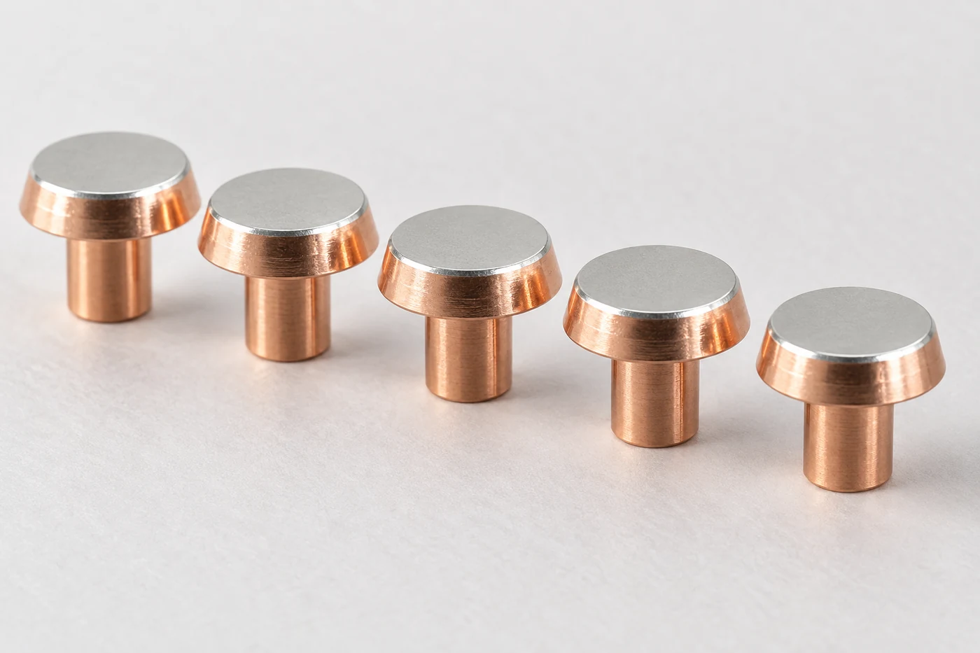
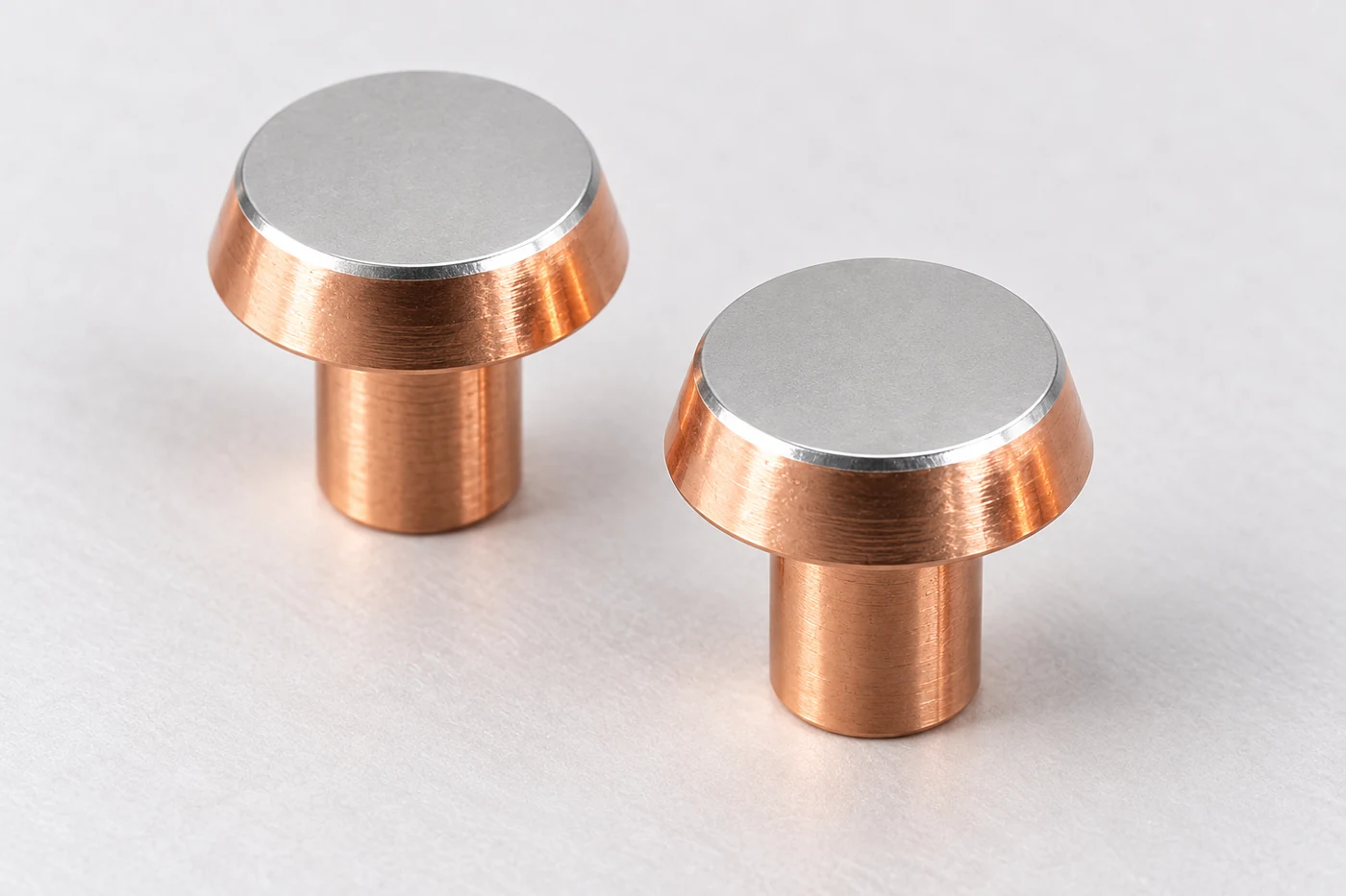
리벳형 전기접점은 머리의 접촉면에서 전류를 주고받고, 하나의 축을 이용해 접점 지지판에 고정하는 구조입니다. 은계 접점재와 구리 모재를 결합한 바이메탈 구조, 전체를 접점재로 만든 솔리드 구조, 그 표면에 추가하는 도금은 서로 다른 사양입니다. 재료 구조와 표면처리를 구분한 뒤 실제 개폐 부하, 접촉력, 온도와 진동 조건에 맞춰 금·은·주석의 적용 부위를 선정해야 합니다.
금·은·주석 도금의 선정 기준
금속의 전기전도도 순서가 접점의 신뢰성 순서는 아닙니다. 금의 중요한 장점은 은보다 높은 전도도가 아니라, 보통의 사용 환경에서 절연성 표면막을 만들기 어렵다는 점입니다. 반대로 주석은 표면이 산화되지만, 정해진 접촉력과 삽입 시 미끄러짐으로 산화막을 뚫어 금속끼리 닿게 만들 수 있습니다.
여기서 접촉력은 두 면을 수직으로 누르는 힘이며, 와이핑은 삽입 과정에서 상대 표면을 따라 미끄러지는 움직임입니다. 두 값은 도금과 함께 정해야 합니다. 새 부품의 도통뿐 아니라 열노화와 반복 삽입을 거친 뒤에도 필요한 힘과 접촉 위치가 유지되는지가 중요합니다.
| 도금 | 주요 적용 접촉부 | 주요 고장 경로 | 선정 시 우선 확인 |
|---|---|---|---|
| 금 Au | 신호용 핀·소켓, 카드 접촉부, 소형 스프링 접촉자 | 얇은 층의 마모 관통, 기공을 통한 하부 금속 부식 | 상대 도금, 금층·하부층 사양, 삽입 수명, 저레벨 저항 |
| 은 Ag | 전력 커넥터, 버스바 분리 접속부, 고전류 도통부 | 황화·오염, 마모, 접촉력 저하와 국부 발열 | 전류·전선·방열 조건, 와이핑, 포장, 온도상승 |
| 주석 Sn | 전장·가전용 프레스 단자, 일반 커넥터, 납땜 영역 | 산화 잔류물 축적, 프레팅, 열노화와 위스커 | 스프링력, 상대 탭 치수, 하우징 구속, 진동 및 열이력 |
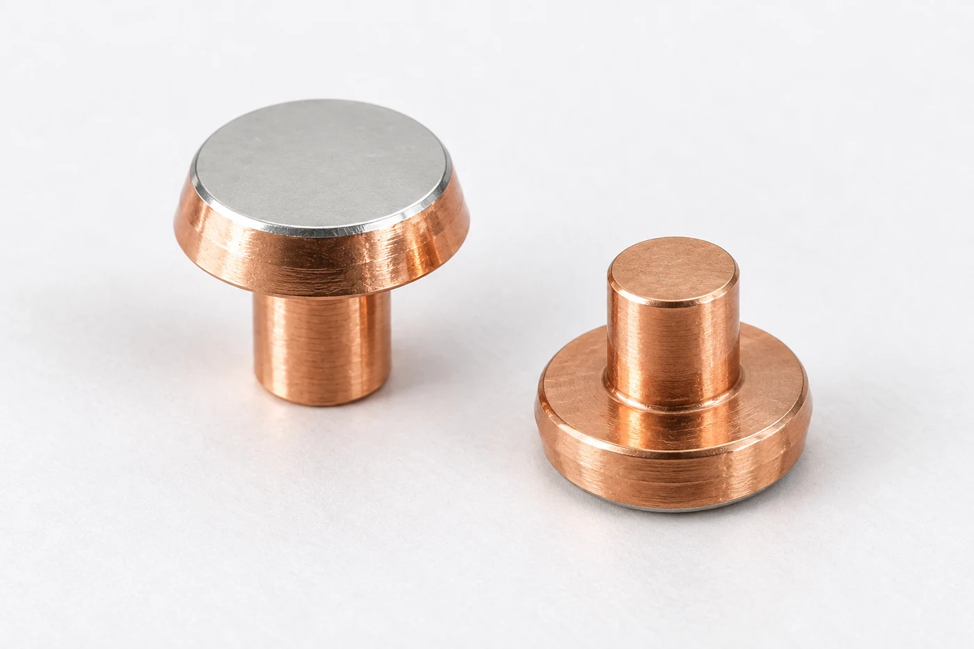
솔리드 리벳은 머리와 축을 접점재로 구성하며, 바이메탈 리벳은 머리의 기능면에 은계 재료를 배치하고 나머지 머리와 축을 구리로 구성하는 방식이 대표적입니다. AgNi·AgSnO₂ 같은 접점 재료층은 개폐 중 아크와 마모를 견디는 역할을 맡습니다. 이 재료층과 표면에 전착하는 금·은도금은 구분해야 합니다. 바이메탈 리벳에도 요구에 따라 별도 도금을 적용할 수 있으며, 은색 외관만으로 솔리드·바이메탈 구조나 도금 여부를 판정할 수는 없습니다.
접촉저항과 전류 경로
겉으로 넓게 맞닿은 두 금속면도 미세하게 보면 일부 돌기에서만 실제로 접촉합니다. 전류는 이 작은 통로로 모였다가 다시 퍼집니다. 이때 생기는 수축저항과 표면막의 저항이 접촉 상태를 좌우하므로, 도금층을 두껍게 하는 것만으로 부족한 접촉력이나 어긋난 접촉 위치를 해결할 수는 없습니다.
전력 접촉부에서는 작은 저항 차이도 열로 나타납니다. 계산 예로, 접촉부 저항이 0.1 mΩ인 상태에서 100 A가 흐르면 그 구간의 발열은 1 W이며, 같은 저항에 200 A가 흐르면 4 W입니다. 특정 제품의 정격을 뜻하는 수치가 아니라 전류 증가에 따른 발열 민감도를 보여주는 예입니다.
발열은 접촉면에만 생기지 않습니다. 전선 압착부, 접촉자 몸체, 스프링 접촉부, 상대 단자까지 전류가 지나가는 모든 구간에 저항이 있습니다. 접촉부 도금을 바꿔도 압착 불량이나 좁은 도체 단면이 남아 있으면 전체 온도는 충분히 낮아지지 않습니다.
따라서 전압을 측정하는 두 위치를 도면에 표시해 비교해야 합니다. 계면만 평가한 저항과 전선·압착부를 포함한 저항은 서로 다른 값입니다. 전선 굵기와 길이, 하우징 내 동시 통전 극수, 주변 온도와 공기 흐름도 고정해야 도금 변경의 효과를 분리할 수 있습니다.
금도금·니켈 하부층과 신호 안정성
금도금은 신호용 리벳 접점 등 작은 부하를 다루는 접촉부에도 적용할 수 있습니다. 리벳에서는 상대 접점이 닿는 머리의 기능면과 지지판에 고정되는 축의 역할이 다릅니다. 솔리드·바이메탈이라는 내부 재료 구조를 먼저 지정하고, 필요한 기능면에 별도의 금층을 설계해야 합니다. 커넥터 핀·소켓 역시 금도금의 주요 적용 예이지만, 그 삽입 수명을 리벳형 개폐 접점의 수명으로 그대로 대입할 수는 없습니다.
낮은 전압·전류의 신호 회로는 표면막을 전기적으로 파괴할 에너지가 작습니다. 경질 금은 산화막 형성이 적고 반복 마찰에 견디도록 설계한 도금이어서 이런 접촉부에 유리합니다. 순도가 높은 연질 금, 경질 금, 얇은 금 플래시를 동일한 수명 사양으로 취급해서는 안 됩니다.
구리합금과 금 사이의 니켈 하부층은 모재 성분의 표면 확산을 억제하고 얇은 금층을 지지합니다. 금층에 기공이 있거나 마찰로 닳으면 하부 금속이 환경에 노출될 수 있습니다. 금층의 평균 두께가 맞더라도 모재의 거친 돌기나 모서리, 실제 마찰 구간에서 층이 불연속이면 안정성이 떨어집니다.
커넥터 도면에 쓰이는 10·30·50 µin은 각각 약 0.254·0.762·1.27 µm입니다. 이들은 실제 상용 도금 옵션에 사용되는 두께이지만, 특정 두께가 모든 제품의 삽입 횟수나 내식 수명을 보장하지는 않습니다. 마찰력·와이핑 길이·상대 표면 거칠기와 환경 시험을 함께 비교해야 합니다.
아크를 받는 금층은 빠르게 손상될 수 있습니다. 신호용으로 검증한 도금을 부하 개폐용으로 그대로 전환하지 말고, 통전 중 삽입·분리 가능 여부와 개폐 정격을 완성품 사양에서 확인해야 합니다. 접점 용착과 발열은 접점 재료뿐 아니라 개폐 동작과 전류 파형을 함께 검토해야 하는 문제입니다.
은계 접점재·은도금과 황화
리벳형 전기접점의 은색 표면은 은계 접점재 자체이거나 추가 은도금의 표면일 수 있습니다. 은계 재료와 구리가 접합된 바이메탈 리벳에도 은도금을 추가하는 제조 방식이 있습니다. 도면에는 접점재 조성·접합 구조와 도금층을 별도 항목으로 적고, 머리의 접촉면과 축의 체결부 중 어느 영역을 처리하는지 명시해야 합니다. 전력 커넥터·버스바의 은도금 접속부는 또 다른 적용 분야이며, 개폐용 리벳 접점과 평가 부하를 구분합니다.
은의 높은 전기·열전도도는 장점이지만, 얇은 은층이 접촉자 전체의 방열 능력을 대신하지는 않습니다. 열은 구리합금 몸체와 연결 도체를 통해 퍼지며, 주변 온도와 하우징의 열적 한계가 허용 전류에 영향을 줍니다. 제조사 전류 저감 곡선도 전선 단면과 단극·다극 구성에 따라 구분해서 읽어야 합니다.
은 표면은 황화수소 등 환경 성분과 반응해 변색될 수 있습니다. 포장용 종이·고무·테이프에서 유래한 성분, 습도, 노출 시간이 영향을 줍니다. 색이 달라졌다는 사실과 도통 기능이 나빠졌다는 사실은 같지 않지만, 접촉력과 와이핑이 부족한 구조에서는 표면막의 영향이 더 커질 수 있습니다.
한 고전류 인터커넥트의 공개 시험에서는 5년·10년 상당의 열노화 전처리와 혼합가스 시험 뒤에도 저항 변화가 해당 제품의 판정 범위에 머물렀습니다. 그 결과는 변색만으로 불량을 판정할 수 없다는 근거이며, 모든 은도금 접점의 변색을 허용한다는 뜻은 아닙니다. 실제 승인에서는 박리·피팅 유무, 접촉저항 변화와 온도상승을 함께 확인합니다.
보관은 황 성분이 적은 포장재와 검증된 변색방지 체계를 사용하고, 접촉면의 지문·오일 오염을 줄이는 방향으로 관리합니다. 변색을 없애기 위해 임의로 연마하면 은층을 소모하거나 잔류물을 남길 수 있습니다. 재세척·재작업 방법도 표면처리 업체와 합의한 절차로 제한하는 편이 좋습니다.
주석도금 적용 부위와 개폐 접점의 구분
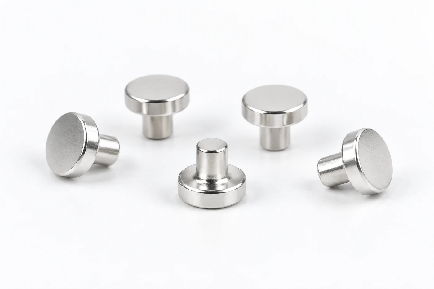
주석도금은 전장·가전의 프레스 단자와 커넥터 접촉부, 납땜 영역에서 널리 활용됩니다. 반면 아크가 발생하는 리벳형 주접점의 은계 재료층을 저렴한 주석도금으로 단순 대체할 수는 없습니다. 같은 스위치 안에서도 부하를 개폐하는 주접점과 전선을 연결하는 단자는 요구 기능이 다릅니다. 주석도금 암단자는 스프링 접촉 빔이 상대 탭을 누르고 삽입 중 표면을 미끄러지며 산화막을 파괴하는 구조를 기준으로 평가합니다.
도체 압착 날개와 피복 또는 실링 지지 날개는 서로 다른 기능을 맡습니다. 앞쪽 압착부는 구리 소선과 전기적·기계적 연결을 형성하고, 뒤쪽 지지부는 케이블 움직임이 접촉부로 전달되는 것을 줄입니다. 압착 불량이나 하우징 내 단자 유격을 도금 두께 증가로 보완할 수는 없습니다.
주석은 비교적 연해 접촉 시 변형되면서 금속 접촉점을 만들 수 있지만, 과한 힘은 삽입력을 높이고 마모를 증가시킵니다. 상대 탭이 두껍거나 모서리가 거칠면 스프링이 과도하게 벌어지거나 도금이 깎일 수 있습니다. 최소·최대 탭 치수에서 삽입력, 인출력과 잔류 접촉력을 각각 확인해야 합니다.
초기 접촉력과 수명 말기의 접촉력도 구분해야 합니다. 열에 오래 노출된 스프링은 응력완화로 가압력이 줄 수 있으며, 여기에 하우징 변형과 케이블 장력이 더해집니다. 소재 조질, 성형 이력과 사용 온도를 함께 검토해야 주석의 경제성을 신뢰성 저하 없이 활용할 수 있습니다.
프레팅과 상대 도금 조합
프레팅은 접촉 상태를 유지한 채 작은 상대운동이 반복되는 현상입니다. 주석이 마찰로 벗겨지고 새 표면이 산화되며, 산화 입자가 빠져나가지 못하고 접촉부에 쌓이면 전류 통로가 줄어듭니다. 완전히 뽑았다 다시 꽂는 동작과 수 µm 수준의 흔들림은 입자의 배출 방식이 달라 같은 마모 시험으로 간주할 수 없습니다.
회전 미끄럼을 조사한 주석도금 모사 접점 연구에서는 실온 대기, 5 mA의 4단자 저항 측정, 접촉력 1 N·6 N과 회전각 2°·6°·10°를 사용했습니다. 6° 조건에서는 가압력이 작은 시편의 저항이 더 일찍 증가했습니다. 이 결과는 힘과 운동 방식이 열화에 영향을 준다는 근거이며, 해당 하중이나 회전 횟수를 실제 단자의 보증값으로 가져올 수는 없습니다.
금도금과 주석도금을 맞물리면 주석이 상대 금 표면으로 이동한 뒤 산화할 수 있습니다. 금 자체가 안정한 금속이더라도 그 위의 주석 산화 입자까지 없어지는 것은 아닙니다. 갈바닉 부식과 마찰에 의한 재료 이동은 다른 현상이므로, 건조한 진동 환경의 문제를 전위차 하나로만 설명해서는 안 됩니다.
설계 변경은 상대 접촉면까지 한 쌍으로 검토합니다. 동일 도금 조합을 우선 검토하되, 이종 도금 조합은 제조사가 제시한 호환성과 실제 내구 조건을 확인해야 합니다. 접점용 윤활제는 마찰·산소 접근을 줄일 수 있지만, 도포량과 재질 적합성, 납땜부 이동 및 잔류물까지 관리해야 합니다.
| 관찰 상황 | 우선 의심할 변수 | 비교할 조건 |
|---|---|---|
| 진동 중에만 순간 단선 | 단자 유격, 접촉력 부족, 산화 잔류물 | 하우징 구속·배선 장력·상대운동 방향 |
| 삽입 횟수 증가 후 저항 상승 | 도금 마모, 상대면 거칠기, 편심 접촉 | 와이핑 길이·하중·마찰 흔적 위치 |
| 금도금품으로 교체해도 재발 | 상대 주석 표면과 재료 이동 | 양쪽 접촉면 도금 및 잔류물 성분 |
접점 성형과 표면처리 공정
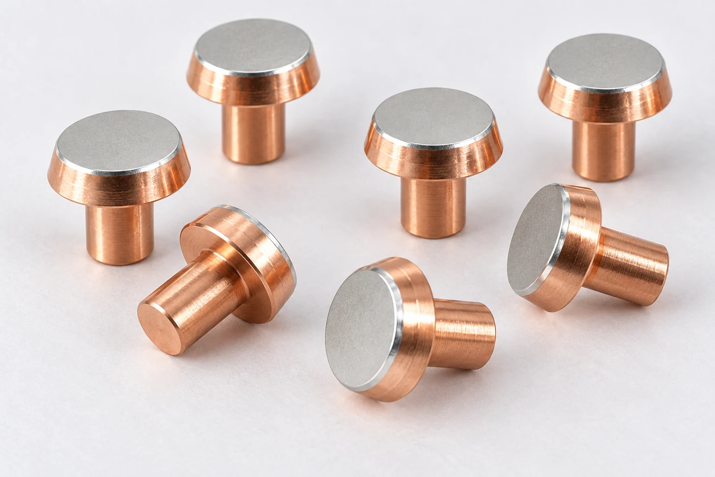
리벳형 접점은 선재의 절단과 냉간 압조로 하나의 머리와 축을 성형하는 방식이 대표적입니다. 바이메탈은 은계 재료와 구리의 접합을 포함하므로 기능층 두께, 접합 계면과 편심을 함께 관리해야 합니다. 머리 지름·높이, 축 지름·길이와 동심도는 지지판의 구멍 및 리벳 체결 조건과 연결됩니다. 접점재의 금속학적 접합을 완료하는 공정과 이후 표면에 얇은 금·은층을 형성하는 도금 공정은 별도로 관리합니다.
프레스 판단자는 리벳 압조와 다른 생산 경로입니다. 선도금은 판재에 표면층을 만든 뒤 절단·성형하는 방식으로, 연속 생산에 유리하지만 새 절단면의 모재 노출과 굽힘부의 층 균열을 확인해야 합니다. 후도금은 성형 뒤 표면처리를 하므로 노출 절단면을 덮을 수 있지만, 깊은 소켓 내부와 좁은 틈의 도금 균일성이 별도 과제가 됩니다.
일반적인 후도금 흐름은 형상 가공과 버 관리, 탈지·세정, 표면 활성화, 승인된 하부층·표면층 형성, 수세·건조, 기능면 검사와 포장으로 이어집니다. 각 층과 전처리 사이의 대기 시간이 길어지거나 세정액이 좁은 틈에 남으면 계면과 후속 품질에 영향을 줄 수 있습니다. 실제 약품과 전류 조건은 모재와 도금 체계에 맞춘 승인 공정으로 관리합니다.
캐리어 스트립 상태의 도금에서는 급송 속도, 전류밀도, 욕 조성·온도, 전극과 접촉부의 위치가 층의 두께와 균일성에 영향을 줍니다. 속도만 올리거나 평균 전류만 맞추기보다 기능면과 모서리의 두께 분포, 밀착·외관을 함께 확인해야 합니다. 공정 이력은 소재 코일, 프레스 로트, 도금 로트와 연결해야 원인을 추적할 수 있습니다.
도금 후 굽힘이나 열처리가 추가되면 하부층의 연성, 층간 확산과 모재의 스프링 특성을 다시 확인합니다. 니켈층도 두꺼울수록 무조건 좋은 것은 아니며, 후성형 조건에서는 균열과 접촉력 변화를 함께 봐야 합니다. 단자 선도금·후도금의 선택은 노출 절단면과 최종 기능면의 위치를 기준으로 검토할 수 있습니다.
선택도금 영역과 조립 공차
선택도금은 서로 맞닿는 영역에는 금 또는 은을, 납땜이나 별도 연결 영역에는 목적에 맞는 다른 표면을 적용하는 방식입니다. 중요한 것은 색의 경계가 아니라, 최악의 조립 공차에서도 실제 접촉점과 와이핑 경로가 필요한 도금 안에 남는지입니다. 기능면을 좁게 잡아 초기 재료비를 낮추더라도 경계가 접촉부에 걸리면 장기 신뢰성을 잃을 수 있습니다.
위치 검토에는 도금 밴드의 흔들림, 프레스 급송 오차, 성형 후 위치 변화, 하우징 삽입 깊이와 상대 부품 공차를 포함합니다. 예를 들어 공차 누적에 따라 접촉점이 이동한다면, 그 이동 범위 전체와 필요한 여유가 도금 영역에 들어가야 합니다. 여유 길이를 모든 단자에 동일한 숫자로 적용하지 말고 실제 치수 사슬에서 정해야 합니다.
도면에는 기능면의 기준점, 도금 시작·끝 위치와 허용 편차, 최소 두께, 경계의 중첩·공백 허용 여부를 함께 표시합니다. 반대면, 버, 절단면과 캐리어 절단 흔적을 어떻게 취급할지도 명시합니다. 얇은 층의 기능 영역은 육안 색상보다 위치 측정과 성분·두께 확인으로 검증하는 편이 확실합니다.
| 관리 대상 | 도면 또는 공정의 정의 | 놓쳤을 때의 문제 |
|---|---|---|
| 접촉 영역 | 상대 접점의 실제 접촉점과 전체 와이핑 경로 | 미도금·이종 도금 경계가 기능면에 진입 |
| 도금 위치 | 제품 기준면에서 시작·끝 위치와 편차 | 급송·성형·조립 오차의 누적 |
| 두께 판정 | 기능면 측정점별 최소값과 필요한 상한 | 평균 합격이나 가장 얇은 위치에서 조기 마모 |
| 후공정 | 굽힘·압착·납땜 후의 상태와 허용 노출부 | 균열, 접촉력 변화, 불필요한 귀금속 소모 |
도금 두께·밀착·표면 결함 검사
XRF는 도금층의 원소 신호를 이용해 두께를 비파괴로 평가하는 방법입니다. 금/니켈/구리처럼 층 구성이 정해져 있어야 적절한 측정 모델을 사용할 수 있습니다. 작은 접촉면에서 조사 영역이 모서리나 다른 재료까지 포함하면 결과가 달라지므로, 빔 크기·측정 거리·시편 방향과 측정 위치를 고정해야 합니다.
리벳 머리의 작은 평면·곡면은 측정점과 시편 방향을 고정하는 지그가 필요합니다. 머리 가장자리나 축까지 XRF 조사 영역에 포함되면 서로 다른 두께·재료의 신호가 섞일 수 있습니다. 바이메탈 접점재층의 두께와 접합 상태는 얇은 추가 도금의 두께와 별도로 판정하며, 필요하면 단면 분석을 병행합니다. 반복 측정과 작업자 간 비교로 실제 공정 편차와 위치 오차를 구분합니다.
단면 분석은 층의 연속성, 국부 두께와 계면 상태를 보는 데 유용하지만 절단·연마 중 층이 번지거나 떨어질 수 있습니다. 외관, XRF 두께와 단면 결과가 충돌하면 시편 준비와 측정 위치부터 대조해야 합니다. 기공 검사는 하부 금속으로 통하는 경로를, 밀착 검사는 층이 떨어지는 경향을 보는 것으로 서로 대체할 수 없습니다.
표면 거칠기·돌기·버는 상대 접점의 마모에도 영향을 줍니다. 완성 외관만 보지 말고 실제 접촉면의 흠집과 도금 돌기, 박리, 오염을 구분해 판정 기준을 마련합니다. 은도금 두께와 수명에서도 두께 숫자와 기능면 위치를 함께 지정하는 것이 중요합니다.
저레벨 저항과 통전·환경 시험
신호 접촉부의 저항은 표면 상태를 바꾸지 않는 낮은 에너지로 먼저 측정합니다. 공개된 커넥터 시험에는 개방전압 20 mV, 시험전류 100 mA의 저레벨 4선식 조건이 사용됩니다. 이 조건을 모든 제품에 자동 적용하기보다 해당 제품 규격을 확인하고, 고전류 시험이나 반복 재삽입으로 표면을 바꾸기 전에 측정 순서를 정해야 합니다.
4선식에서는 전류를 흘리는 연결과 전압을 읽는 연결을 분리해 리드선 저항의 영향을 줄입니다. 미세 저항을 비교할 때는 검출점 위치와 열기전력, 안정화 시간도 관리합니다. 진동 중 순간 접촉 불량이 문제라면 시험 전후 평균 저항뿐 아니라 시간에 따른 단속과 검출 가능한 최소 지속시간을 기록해야 합니다.
전력 접촉부는 정격 조건의 전류를 흘리며 주위 대비 온도상승과 가장 뜨거운 지점의 절대온도를 모두 확인합니다. 시험 중 저항 상승과 접촉력 저하가 동반되는지 보면 표면 열화와 구조 문제를 구분하는 데 도움이 됩니다. 합격 온도와 저항 변화량은 하우징·전선·접촉자 사양에 근거해 시험 전에 정합니다.
| 시험군 | 재현할 조건 | 측정 결과와 판단 |
|---|---|---|
| 반복 삽입 | 상대 부품, 횟수, 속도, 정렬, 무부하·부하 상태 | 저항 추이, 삽입력·인출력, 기능면 마모 관통 |
| 진동·열사이클 | 하우징 고정, 배선 지지, 방향, 온도 범위 | 순간 단속, 저항 변화, 접촉력 및 단자 유격 |
| 열노화 | 실제 부품 온도와 노출 시간, 조립 상태 | 스프링 응력완화, 층간 반응, 잔류 접촉력 |
| 부식·혼합가스 | 가스 종류·농도, 온습도, 노출 시간, 결합 여부 | 표면 변화와 저레벨 저항의 상관관계 |
| 통전 발열 | 전선 단면·길이, 동시 통전 극수, 주위 온도 | 국부 최고온도, 온도상승, 전압강하와 안정화 |
염수분무 시험 하나로 실내 황화 환경이나 프레팅 내구를 대신할 수 없습니다. 각각 노출 매체와 고장 메커니즘이 다르기 때문입니다. 미결합 보관 뒤 처음 접촉하는 상황과 결합된 채 노화하는 상황도 나누어 시험해야 실제 사용 순서를 반영할 수 있습니다.
불량 형태와 원인 분리
불량 분석은 원래 표면을 보존한 상태에서 시작합니다. 세척하거나 여러 번 재삽입하면 산화 잔류물과 접촉 흔적이 달라져 원인을 놓칠 수 있습니다. 먼저 발생 조건과 저항·온도를 기록하고, 비파괴 관찰 뒤 필요한 시편만 분해·단면 분석하는 순서가 유리합니다.
| 불량 양상 | 구분할 원인 | 확인 근거 |
|---|---|---|
| 금색 표면 일부 소실 | 마모 관통, 오염, 도금 불균일 | 마찰 경로와 층별 두께·성분 |
| 은 접촉면 변색 | 표면 황화, 심한 부식, 취급 오염 | 피팅·박리 유무와 저항·온도상승 |
| 주석 접촉부 회색·검은 잔류물 | 산화 마모분, 외부 오염 | 잔류물 성분, 상대운동 및 접촉력 |
| 국부 과열 | 계면 저항, 압착 불량, 도체 단면 부족 | 구간별 전압강하와 열 발생 위치 |
| 전기적 단락 | 금속 이물, 주석 위스커, 전기화학적 이동 | 성장 형태, 간격, 습도·바이어스 및 표면 성분 |
주석 위스커는 마찰로 생긴 가루와 다른 현상입니다. 도금 내부 응력, 모재와의 금속간화합물 형성, 외부 압축과 후성형 등이 성장 위험에 영향을 줄 수 있습니다. 수분과 전기장이 작용해 표면을 따라 성장하는 수지상 석출물과도 구분해야 하며, 니켈 하부층이나 무광 주석만으로 위험이 완전히 사라진다고 단정해서는 안 됩니다.
재발 방지는 관찰된 원인에 연결해야 합니다. 기능면 마모라면 두께·경도·상대 거칠기를, 미세 운동이라면 하우징과 배선 구속을, 가압력 저하라면 스프링 소재·성형·열이력을 우선 수정합니다. 도금 변경 전후의 시편을 동일한 시험 순서로 비교해야 개선 효과를 판단할 수 있습니다.
도면 사양과 제조비용
발주 사양은 도금 금속, 하부층, 기능면의 두께와 위치뿐 아니라 상대 부품과 사용 조건까지 연결되어야 합니다. 상대 탭·핀의 재료와 표면, 최소·최대 치수, 삽입 횟수, 전류·듀티, 진동과 환경 조건을 함께 제공하면 제조 공정과 검증 항목을 구체적으로 정할 수 있습니다.
비용은 금속 사용량 외에도 도금 면적, 선택도금 위치 정밀도, 급송 속도, 치구·마스킹, 검사 접근성과 불량률에 영향을 받습니다. 동일한 면적에서 두께를 두 배로 하면 도금 금속의 이론적 사용량은 두 배가 되지만, 전처리·설비·검사비까지 모두 두 배가 되는 것은 아닙니다. 따라서 전체 금도금과 선택도금의 견적은 같은 기능 수명과 검사 조건으로 비교해야 합니다.
원가를 줄일 때는 먼저 불필요한 귀금속 면적과 중복 공정을 살펴봅니다. 기능면 축소는 공차 검토 후에, 두께 감소는 마모와 내환경 검증 후에 판단합니다. 주석으로 바꾸면서 상대 접점, 접촉력과 하우징 구조를 그대로 두는 변경은 재검증 비용과 불량 위험을 함께 포함해야 합니다.
샘플 승인에서는 초기 저항, 힘과 외관만 받지 말고 도금 측정 위치, 사용한 상대 부품, 시험 순서, 로트 이력을 함께 보관합니다. 양산 변경 시에는 소재·조질, 전처리, 하부층, 표면층, 윤활제와 포장 변경이 검증 범위에 미치는 영향을 검토합니다. 이 연결이 있어야 가격 비교가 장기적인 품질과 납기 판단으로 이어집니다.
접촉자 모재의 탄성과 열적 안정성은 인청동·베릴륨동·황동의 차이와 함께 검토할 수 있습니다. 개폐용 재료 구조는 전기접점 재질에서 구분하고, 실제 도면과 사용 조건에 따른 제작 검토는 ID METAL 개발의뢰로 연결하실 수 있습니다.
English Technical Overview
Electrical contact plating is a functional layer that controls oxidation, corrosion and repeated friction so that current can flow reliably. Gold offers stable low-level signal transmission, silver supports low-resistance power connections, and tin provides economical terminal production and solderability. Even with the same finish, however, service life changes substantially with contact force, the mating surface, temperature and friction history.
A rivet electrical contact carries current through the working face of its head and uses one shank for attachment to a contact carrier. A bimetal construction joining silver-based contact material to copper, a solid construction made from contact material throughout, and an additional plated finish are different specifications. Distinguish material construction from surface treatment before selecting where gold, silver or tin belongs, based on the actual switching load, contact force, temperature and vibration.
Selection Criteria for Gold, Silver and Tin
The ranking of bulk electrical conductivity is not a ranking of contact reliability. The important advantage of gold is not higher conductivity than silver, but its resistance to forming insulating surface films in ordinary service environments. Tin oxidizes, yet controlled normal force and sliding during insertion can break through the film and establish metal-to-metal contact.
Normal contact force presses the two surfaces together. Wiping is their relative sliding motion during insertion. Both must be specified together with the finish. The requirement is not merely continuity in new parts: sufficient force and the correct contact location must remain after thermal aging and repeated mating.
| Finish | Typical contact applications | Principal degradation paths | Priority checks |
|---|---|---|---|
| Gold, Au | Signal pins and sockets, card contacts and small spring contacts | Wear-through of thin layers; corrosion of underlying metal through pores | Mating finish, gold and underplate specifications, mating endurance and low-level resistance |
| Silver, Ag | Power connectors, separable busbar joints and high-current connections | Tarnish and contamination, wear, force loss and localized heating | Current, wire and cooling conditions; wiping, packaging and temperature rise |
| Tin, Sn | Stamped automotive and appliance terminals, general connectors and soldering areas | Oxide-debris accumulation, fretting, thermal aging and whiskers | Spring force, mating-tab dimensions, housing restraint, vibration and thermal history |
A solid contact rivet uses contact material for both head and shank. A common bimetal construction places silver-based material on the working face, with copper forming the remainder of the head and the shank. Contact-material layers such as AgNi or AgSnO₂ provide resistance to switching arcs and wear. They must be distinguished from electrodeposited gold or silver finishes. Bimetal rivets can also receive an additional plated finish when required. A silver-colored appearance alone does not establish solid or bimetal construction, or whether plating is present.
Contact Resistance and the Current Path
Although two metal surfaces appear to touch over a broad area, actual contact occurs at a limited number of microscopic asperities. Current converges into these small paths and then spreads out again. The resulting constriction resistance and the resistance of surface films govern the interface, so thicker plating alone cannot correct inadequate force or a misplaced contact zone.
In a power connection, even a small resistance difference produces heat. As a calculation example, a contact resistance of 0.1 mΩ dissipates 1 W at 100 A and 4 W at 200 A if the resistance remains unchanged. These values illustrate sensitivity to current; they are not ratings for any particular product.
Heat is generated throughout the current path, including the wire crimp, contact body, spring interface and mating terminal. A plating change cannot adequately reduce the total temperature if a defective crimp or undersized conductor section remains.
The two voltage-sensing locations should therefore be marked on the drawing. Resistance measured across an interface is different from a value that includes wire and crimp sections. Wire size and length, the number of simultaneously energized poles, ambient temperature and airflow must remain controlled to isolate the effect of a finish change.
Gold, Nickel Underplate and Signal Stability
Gold plating can also be applied to low-load interfaces such as signal contact rivets. On a rivet, the working head face that meets the opposing contact has a different function from the shank attached to the carrier. Specify the solid or bimetal internal construction first, then define a separate gold layer on the required functional surface. Connector pins and sockets are another major application, but their mating-cycle life cannot be transferred directly to the switching life of rivet contacts.
Low-voltage, low-current signal circuits have little energy available to electrically disrupt surface films. Hard gold combines resistance to oxidation with a finish designed for repeated sliding, making it useful for these interfaces. High-purity soft gold, hard gold and a thin gold flash must not be treated as equivalent endurance specifications.
A nickel underplate between the copper alloy and gold limits diffusion of base-metal constituents toward the surface and supports the thin gold layer. Pores or wear can expose underlying metal to the environment. Even if average gold thickness meets the specification, discontinuities over rough substrate asperities, edges or the actual wear path can undermine stability.
The 10, 30 and 50 µin options seen on connector drawings correspond to approximately 0.254, 0.762 and 1.27 µm. These are real commercial plating options, but no one thickness guarantees a universal mating-cycle count or corrosion life. Friction force, wipe length, mating-surface roughness and environmental tests must be considered together.
Arcing can rapidly damage a gold layer. A finish qualified for signal service should not be transferred directly to load switching. Verify live mating or unmating capability and switching ratings in the finished-product specification. Contact welding and heating require examination of switching motion and current waveform as well as contact material.
Silver Contact Materials, Silver Plating and Tarnish
The silver-colored surface of a rivet contact may be the silver-based contact material itself or an additional silver-plated finish. Bimetal rivets joining silver-based material to copper can also receive silver plating. Drawings should specify contact-material composition and bonded construction separately from the plated layer, including whether treatment covers the working head face, the attachment shank or other areas. Silver-plated power connectors and busbar joints are different applications and require different test loads from switching rivets.
Silver offers high electrical and thermal conductivity, but a thin silver layer does not replace the heat-spreading capacity of the complete contact. Heat flows through the copper-alloy body and connected conductor, while ambient conditions and the housing thermal limit affect allowable current. Manufacturer derating curves must be read for the applicable wire cross-section and single- or multipole configuration.
Silver can discolor through reactions with environmental constituents such as hydrogen sulfide. Packaging paper, rubber and tape, along with humidity and exposure time, can contribute. A change in color is not the same as a loss of electrical function, although a surface film may have greater consequences in a design with insufficient force or wiping.
In a published high-power interconnect test, resistance changes remained within that product’s acceptance limits after thermal preconditioning described as equivalent to five and ten years, followed by mixed-flowing-gas testing. This supports evaluating more than appearance alone; it does not justify accepting all tarnished silver contacts. Qualification should also assess pitting, delamination, resistance change and temperature rise.
Storage controls should use low-sulfur packaging and a validated anti-tarnish approach while minimizing fingerprints and oil on functional surfaces. Arbitrary polishing to remove discoloration can consume silver or leave residue. Cleaning and rework should follow procedures agreed with the surface-treatment supplier.
Tin-Plating Applications and Switching Contacts
Tin plating is widely used on stamped automotive and appliance terminals, connector interfaces and soldering areas. It cannot simply replace the silver-based material layer of an arcing main contact rivet as a lower-cost finish. Even within one switch, the load-switching contacts and the wire-connection terminals have different functions. A tin-plated female terminal should be evaluated as a structure in which spring beams press against the mating tab and sliding during insertion disrupts the oxide film.
Conductor-crimp wings and insulation- or seal-support wings serve different purposes. The forward crimp establishes electrical and mechanical attachment to the copper strands. The rear support reduces transmission of cable movement into the contact interface. Increasing plating thickness cannot compensate for a defective crimp or a loose terminal in its housing.
Relatively soft tin can deform to establish metallic contact spots, but excessive force increases insertion force and wear. An oversized tab or a rough edge may overstress the spring or scrape away plating. Insertion force, withdrawal force and residual contact force should be checked at both minimum and maximum tab dimensions.
Initial contact force must also be distinguished from end-of-life force. Prolonged heat exposure can reduce spring force through stress relaxation, compounded by housing distortion and cable tension. Alloy temper, forming history and service temperature must be reviewed together to retain the cost benefits of tin without sacrificing reliability.
Fretting and Mating-Finish Combinations
Fretting is repeated small relative motion while the surfaces remain in contact. Tin wears away, newly exposed surfaces oxidize, and trapped oxide debris can accumulate until current paths are restricted. Complete unmating and remating differs from movement of only a few micrometres because debris removal is different; they are not interchangeable wear tests.
A study of rotational microsliding in model tin-plated contacts used room-temperature air, four-terminal resistance measurement at 5 mA, normal forces of 1 N and 6 N, and rotation angles of 2°, 6° and 10°. Under the 6° condition, resistance increased earlier for the lower-force specimens. This demonstrates the influence of force and motion mode, but the loads or cycle counts are not transferable as guarantees for a real terminal.
When gold mates with tin, tin can transfer onto the gold surface and subsequently oxidize. The chemical stability of gold does not remove tin-oxide debris deposited on top of it. Galvanic corrosion and friction-driven material transfer are different phenomena, so a problem in a dry vibrating interface should not be explained solely by electrochemical potential differences.
A design change must evaluate the two mating surfaces as a pair. Matched finishes are a useful starting point, while mixed finishes require manufacturer compatibility information and validation under the actual endurance conditions. Contact lubricant may reduce friction and oxygen access, but its quantity, material compatibility, migration toward soldering areas and residues must also be controlled.
| Observed behavior | Variables to examine first | Conditions to compare |
|---|---|---|
| Momentary discontinuity only during vibration | Terminal play, inadequate force and oxide debris | Housing restraint, cable tension and direction of relative motion |
| Resistance increases with mating cycles | Plating wear, mating roughness and off-center contact | Wipe length, force and location of wear tracks |
| Failure returns after changing one part to gold | Transfer from the mating tin surface | Finishes on both sides and debris composition |
Contact Forming and Surface-Treatment Processes
Contact rivets are commonly produced by cutting wire and cold heading a single head and shank. Bimetal production also involves joining silver-based material to copper, so functional-layer thickness, the bonded interface and eccentricity require control. Head diameter and height, shank diameter and length, and concentricity must be coordinated with the carrier hole and riveting conditions. Metallurgical joining of the contact materials and subsequent deposition of a thin gold or silver finish are separate manufacturing operations.
Stamped sheet terminals follow a different production route from cold-headed rivets. Preplating applies the surface layer to strip before cutting and forming. It supports continuous production, but newly exposed cut edges and cracking at bends require assessment. Postplating treats the formed part and can cover exposed cut surfaces, while uniformity inside deep receptacles and narrow gaps becomes a separate challenge.
A typical postplating sequence includes geometry production and burr control, degreasing and cleaning, surface activation, deposition of the approved underplate and top layer, rinsing and drying, functional-surface inspection and packaging. Excessive delays between stages or retained cleaning solution in narrow gaps may compromise the interface and later quality. Chemicals and electrical conditions must be controlled through a process approved for the substrate and coating system.
For carrier-strip plating, feed speed, current density, bath composition and temperature, and electrode positioning affect thickness and uniformity. Increasing speed or maintaining average current is not enough: thickness distribution at functional faces and edges, adhesion and appearance must be checked together. Material-coil, stamping-lot and plating-lot records need to remain connected for traceability.
Additional bending or heat treatment after plating requires reassessment of underplate ductility, interdiffusion and substrate spring properties. Thicker nickel is not automatically better; postforming may introduce cracking or force changes. The choice between terminal preplating and postplating should reflect exposed cut edges and the final functional-surface location.
Selective-Plating Zones and Assembly Tolerances
Selective plating places gold or silver on the mating area and an appropriate alternative finish on soldering or other connection areas. The essential question is whether the real contact point and complete wipe path remain within the required finish under worst-case assembly tolerances. Reducing the functional band may lower initial material cost but compromise life if the boundary enters the interface.
Position analysis should include plating-band variation, press-feed error, changes after forming, housing insertion depth and mating-part tolerances. When the accumulated tolerances move the contact point, the entire movement range plus the necessary margin must remain inside the plated zone. Margin length should come from the actual dimensional chain, not a universal number for every terminal.
Drawings should define the functional-area datum, start and end positions with tolerances, minimum thickness, and whether boundary overlap or gaps are permissible. They should also address the reverse face, burrs, cut edges and carrier-separation marks. Position measurement and composition or thickness verification are more dependable than visible color alone for thin functional layers.
| Controlled feature | Drawing or process definition | Consequence if omitted |
|---|---|---|
| Contact area | Actual contact point and complete wiping path | Unplated areas or mixed-finish boundaries enter the interface |
| Plating position | Start, end and deviation from the product datum | Accumulated feed, forming and assembly error |
| Thickness acceptance | Minimum at defined functional points and any necessary upper limit | Acceptable average but early wear at the thinnest location |
| Subsequent operations | Condition after bending, crimping or soldering; permitted exposure | Cracking, force changes and unnecessary precious-metal consumption |
Thickness, Adhesion and Surface-Defect Inspection
X-ray fluorescence, or XRF, evaluates coating thickness nondestructively using elemental signals. An appropriate measurement model requires a defined layer stack, such as gold over nickel on copper. Results can change if the illuminated area includes an edge or another material. Beam size, measurement distance, specimen orientation and measurement location must therefore be controlled.
The small flat or curved face of a rivet head requires a fixture that fixes the measurement point and orientation. If the XRF beam includes a head edge or the shank, signals from different thicknesses or materials can be mixed. Assess the bimetal contact-material layer and its bond separately from the thickness of any thin additional plating, using cross-sections where necessary. Repeat measurements and operator comparisons distinguish real process variation from positioning error.
Cross-sections reveal layer continuity, local thickness and interface condition, but cutting and polishing can smear or detach a layer. If appearance, XRF and cross-sectional results conflict, compare specimen preparation and locations first. Porosity testing examines paths through to underlying metal, whereas adhesion testing examines separation tendency; one cannot replace the other.
Roughness, nodules and burrs can also accelerate wear on the mating contact. Acceptance criteria should distinguish scratches, plating protrusions, delamination and contamination on the actual contact surface rather than judging overall appearance alone. In silver-plating thickness and service life, the functional location matters as much as the thickness value.
Low-Level Resistance, Current and Environmental Tests
Signal-contact resistance should first be measured at low energy that does not alter the surface. Published connector tests include a low-level four-wire condition of 20 mV open-circuit voltage and 100 mA test current. Confirm the applicable product specification instead of automatically applying these settings to every part. Establish the test order before high-current tests or repeated remating modify the interface.
Four-wire measurement separates current connections from voltage-sensing connections to reduce lead-resistance effects. Comparing very small resistances also requires control of sensing locations, thermal electromotive forces and stabilization time. If brief vibration-induced discontinuities are the concern, record interruptions over time and the minimum detectable event duration, not only average resistance before and after testing.
Power-contact tests should measure both rise above ambient and absolute temperature at the hottest location while carrying the specified current. Simultaneous resistance increase and force loss can help separate surface degradation from structural problems. Temperature limits and allowable resistance change must be established before testing from the housing, wire and contact specifications.
| Test group | Conditions to reproduce | Measurements and assessment |
|---|---|---|
| Repeated mating | Mating part, cycles, speed, alignment and loaded or unloaded operation | Resistance trend, insertion and withdrawal forces, functional-layer wear-through |
| Vibration and thermal cycling | Housing mounting, cable support, direction and temperature range | Transient discontinuity, resistance change, force and terminal play |
| Thermal aging | Actual part temperature, exposure time and assembled condition | Spring relaxation, layer reactions and residual contact force |
| Corrosion and mixed flowing gas | Gas species and concentration, temperature, humidity, duration and mating state | Relationship between surface changes and low-level resistance |
| Current-induced heating | Wire cross-section and length, energized poles and ambient temperature | Local peak temperature, temperature rise, voltage drop and stabilization |
A salt-spray test cannot by itself substitute for indoor sulfur exposure or fretting endurance because the media and failure mechanisms differ. Storage while unmated followed by first connection should also be distinguished from aging while mated so that the test reflects the real sequence of use.
Separating Failure Symptoms and Causes
Failure analysis should begin with the original surface preserved. Cleaning or repeated remating may change oxide debris and contact tracks and obscure the cause. Record the operating conditions, resistance and temperature first, then use nondestructive observation before disassembling or sectioning selected specimens.
| Failure appearance | Causes to distinguish | Supporting evidence |
|---|---|---|
| Local loss of the gold-colored surface | Wear-through, contamination or nonuniform plating | Wear path, layer thickness and composition |
| Discolored silver interface | Surface tarnish, severe corrosion or handling contamination | Pitting or delamination, resistance and temperature rise |
| Gray or black residue on tin contacts | Oxidized wear debris or external contamination | Debris composition, relative motion and contact force |
| Localized overheating | Interface resistance, defective crimp or inadequate conductor section | Segment-by-segment voltage drop and heat location |
| Electrical short circuit | Metal debris, tin whiskers or electrochemical migration | Growth morphology, spacing, humidity, bias and surface composition |
Tin whiskers differ from friction-generated powder. Internal plating stress, intermetallic formation with the substrate, external compression and postforming can affect growth risk. They must also be distinguished from dendritic deposits associated with moisture and an electric field. Nickel underplating or matte tin alone should not be claimed to eliminate whisker risk.
Corrective action must address the observed mechanism. For functional-surface wear, review thickness, hardness and mating roughness; for micromotion, review housing and cable restraint; for force loss, review spring material, forming and thermal history. Compare the original and modified parts in the same test sequence to establish whether the change is effective.
Drawing Requirements and Manufacturing Cost
Procurement specifications should connect plating metal, underplate, functional thickness and location to the mating component and service conditions. Providing mating-tab or pin material and finish, dimensional limits, mating cycles, current and duty, vibration and environment enables a specific manufacturing and validation plan.
Cost depends not only on deposited metal but also on plated area, selective-plating positional accuracy, line speed, fixtures and masking, inspection access and rejection rate. Doubling thickness over an unchanged area doubles theoretical deposited-metal consumption, but it does not double all pretreatment, equipment and inspection costs. Overall and selective gold-plating quotations must therefore be compared at equivalent functional life and inspection requirements.
Cost reduction should first examine unnecessary precious-metal area and duplicated processing. Reduce functional coverage only after tolerance analysis, and reduce thickness only after wear and environmental validation. Changing to tin while keeping the mating finish, force and housing unchanged requires consideration of requalification cost and failure risk.
Sample approval records should include more than initial resistance, force and appearance. Retain thickness-measurement locations, the mating parts used, test order and lot history. Production changes to substrate or temper, pretreatment, underplate, topcoat, lubricant or packaging should be reviewed for their effect on the qualification scope. These connections make a price comparison meaningful for long-term quality and delivery.
The elasticity and thermal stability of the contact substrate can be considered alongside phosphor bronze, beryllium copper and brass. Distinguish switching-material structures in electrical contact materials, and use ID METAL development inquiries for a manufacturing review based on actual drawings and service conditions.
추가 정보
검색엔진용 요약
전기접점 도금은 금·은·주석의 특성과 접촉 구조를 함께 선정해야 합니다. 신호 접촉자의 저레벨 도통, 은도금 전력 접촉자의 발열·황화, 주석도금 판단자의 프레팅을 구분하고 하부층·선택도금·두께 검사와 수명 시험을 도면 및 발주 조건으로 연결합니다.
핵심 포인트 정리
- 도금층과 AgNi·AgSnO₂ 등 개폐용 접점재를 구분합니다.
- 금은 경질·연질·플래시와 니켈 하부층의 역할을 구분해 선정합니다.
- 은도금은 변색 외관과 전기적 기능을 저항·온도상승으로 나누어 판정합니다.
- 주석은 상대 탭 치수, 수명 말기 접촉력과 미세 운동을 함께 검증합니다.
- 선택도금 영역은 전체 와이핑 경로와 조립 공차를 포함해야 합니다.
- 두께·밀착·기공 검사와 완성 접점의 환경·통전 시험을 연결합니다.
FAQ
금도금으로 바꾸면 접촉저항이 항상 낮아집니까?
표면막이 원인이면 개선될 수 있지만 압착 불량, 스프링력 저하나 접촉 위치 오류까지 해결하지는 못합니다. 구간별 전압강하와 상대 접점 상태를 확인한 뒤 도금 변경 효과를 비교해야 합니다.
은도금 접촉자와 은합금 접점 팁은 무엇이 다릅니까?
은도금 접촉자는 구리합금 등의 표면에 은층을 형성한 구조입니다. 은합금 접점 팁은 접점재 자체가 개폐와 아크를 견디는 기능을 맡으며 접합부와 재료 조성까지 별도로 설계합니다.
도금 두께는 어느 위치에서 측정해야 합니까?
상대 부품이 실제로 닿고 미끄러지는 기능면을 우선 지정합니다. 모서리·곡면·깊은 소켓은 도금과 측정 편차가 커질 수 있어 측정점, 시편 방향, XRF 조사 영역과 보완 단면 검사를 함께 정합니다.
주석도금 단자가 진동 중에만 불안정한 이유는 무엇입니까?
미세 운동에 의해 주석 마모분과 산화물이 축적되거나 접촉력이 부족할 수 있습니다. 시험 전후 도통만 확인하지 말고 진동 중 단속, 하우징 유격, 배선 장력과 접촉 흔적을 함께 확인해야 합니다.
금도금과 주석도금을 맞물려 사용할 수 있습니까?
한쪽 도금만 바꾸어 승인하는 방식은 피해야 합니다. 주석의 금 표면 이동과 산화 잔류물 축적을 고려해 제조사 호환성, 접촉력, 윤활 조건과 실제 내환경·내구 시험으로 해당 조합을 평가해야 합니다.
도금 비용을 줄일 때 먼저 검토할 항목은 무엇입니까?
불필요한 귀금속 면적, 중복 공정, 과도한 위치 정밀도와 검사 난이도를 먼저 살펴봅니다. 기능면 범위를 줄이거나 두께를 낮추는 변경은 조립 공차와 내구·부식 검증을 통과한 뒤 반영합니다.
관련 주제 확장 설명
접촉력과 스프링 소재
열노화 후의 가압력이 부족하면 도금의 장점도 유지하기 어렵습니다. 모재의 조질과 성형 이력, 상대 탭 치수, 하우징 구속을 함께 검토해야 표면처리와 구조 설계가 연결됩니다.
도금 검사와 측정 재현성
기능면보다 큰 XRF 조사 영역이나 매번 달라지는 곡면 방향은 두께 비교를 흐릴 수 있습니다. 지그·기준 시편·측정점 정의와 반복성 평가를 통해 실제 공정 변동과 측정 오차를 구분합니다.
설계 변경과 양산 승인
도금 체계의 변경은 상대 부품과 시험 순서, 포장 조건까지 영향을 줄 수 있습니다. 기존 승인품과 변경품을 동일한 조건으로 비교하고 소재·도금·조립 로트 이력을 함께 보관합니다.
내부 링크
접점 팁의 재료 거동은 전기접점 재질과 적용 특성에서 함께 검토할 수 있으며, 은도금의 기능면 두께 기준은 은도금 두께와 접점 수명에서 더 구체적으로 확인할 수 있습니다.
단자 제작의 공정 경계는 단자 선도금·후도금 차이와 연결됩니다. 실제 도면과 사용 조건에 따른 검토는 ID METAL 개발의뢰를 통해 상담하실 수 있습니다.