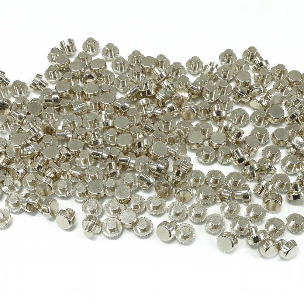
SJ06 (Ag–SnO₂–In₂O₃) 전기접점 재료
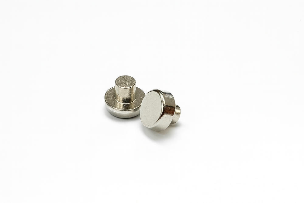
SJ06 (Ag–SnO₂–In₂O₃) 전기접점 재료
SJ06 전기접점은 은(Ag)을 모체로 하고 주석산화물(SnO₂)을 분산상으로 포함하며 인듐 산화물(In₂O₃)을 약 2% 수준으로 첨가한 은계 복합 재료이다.
이 구조는 아크 발생 시의 열·기계적 부담을 견디고, 스위칭 반복 환경에서 안정적인 접촉 특성을 유지하도록 설계되어 있다.
Ag–SnO₂–In₂O₃ 계열 재료는 Cd-free 구조를 기본으로 하여 환경 규제를 충족하며, 저전압 스위치·릴레이·컨택터 등에서 안정적인 성능을 유지하기 위한 대체재로 자리잡고 있다.
재료 구성 및 미세조직
화학 조성
SJ06 계 전기접점은 아래와 같은 구성 범위를 갖는다.
Ag: 약 82–90 wt%
SnO₂: 약 8–14 wt%
In₂O₃: 약 2–4 wt%
이 조성은 Ag 매트릭스의 높은 전기전도도와 SnO₂의 고경도·내열 특성, In₂O₃의 미세조직 안정화 효과를 조합한 구조이다.
SnO₂@In₂O₃ 복합 구조
고에너지 볼 밀링 또는 내부 산화 공정을 활용해 SnO₂ 주변에 In₂O₃가 결합한 형태의 복합 분산 구조(SnO₂@In₂O₃)가 형성된다.
이 구조는 다음 특성을 부여한다.
입자 크기 미세화
Ag와 산화물 계면의 결합력 향상
입자의 균일 분산
아크 시 재료 비산(minimal spattering) 억제
제조 공정
SJ06 계 재료는 주로 아래의 방식으로 생산된다.
내부 산화(Internal oxidation) 기반 산화 분산 형성
분말야금 공정(압축, 소결, 재소결)
고에너지 볼 밀링 + 반응 합성(Reaction synthesis)
필요 시 나노 산화물 코팅 적용
이 공정들은 고밀도·저기공의 미세조직을 형성하며 아크·마모 저항성 개선을 위한 기반이 된다.
적용 분야
SJ06 전기접점은 전기적·환경적 요구 조건이 높은 다양한 시스템에서 활용된다.
저전압 스위치 및 보호장치
MCB, MCCB
산업용 컨택터
범용 릴레이
개폐 빈도가 높은 장치에서의 아크와 재료 마모를 최소화하며, 장기 동작 시 접촉 저항 변화를 억제하는 데 적합하다.
자동차 및 전기차(EV)용 릴레이
파워 릴레이
BMS 스위칭 접점
DC 컨택터
인버터 주변 보조 접점
DC 전류 환경에서 재료 편이(material transfer)가 적고, 반복 스위칭에 따른 용착 현상을 억제하여 전기차의 고전압 시스템 안정성에 유리하다.
가전·산업 자동화 장비
모터 제어용 접촉기
가전용 전자 릴레이
PLC 기반 자동화 제어 장비
습도·온도 변화가 존재하는 산업 환경에서도 접촉 특성이 안정적으로 유지된다.
재생 에너지 및 전력전자
태양광 인버터
ESS 시스템 스위칭
고주파 전력전자 회로
고주파 스위칭 환경에서 아크 에너지 변동 폭이 작고 절연 신뢰도가 우수한 특성이 요구되는 곳에 적합하다.
사용 환경 및 성능
전기적 성능
비저항은 약 3.3–3.5 μΩ·cm 범위로 유지될 수 있다.
접촉 저항은 스위칭 횟수 증가에도 안정적으로 유지되며 변동 폭이 작다.
아크 발생 시 Ag의 과도한 용융·비산이 억제되고, SnO₂·In₂O₃ 복합 분산층이 구조적 안정성을 제공한다.
기계적 성능
고밀도 소결 구조로 인해 높은 경도(HV 700 전후) 확보
산화물 입자의 균일 분산으로 균열 전파 억제
반복 기계 충격과 진동 환경에서도 접점 구조 유지
열·환경적 안정성
SnO₂와 In₂O₃의 높은 열안정성으로 인해 온도 변화에 따른 재료 변형이 적다.
Cd-free 구조로 환경 규제 대응에 유리하다.
장기 사용 환경에서 산화층 증가 속도가 완만하여 수명 유지에 유리하다.
SJ06 전기접점
아크 침식 저감
SnO₂와 In₂O₃ 복합 분산 구조는 아크 에너지 전달을 안정화시키며 침식량을 크게 낮춘다.
낮고 안정된 접촉 저항
내부 산화와 고밀도 소결 구조가 계면 결합력과 전기전도도를 유지한다.
용착 저항성 향상
DC 스위칭 환경에서의 재료 이동과 국부 용착 발생을 효과적으로 억제한다.
기계적 강도·피로 내구성 향상
산화물 분산 강화 효과로 반복 스위칭 사이클에서의 균열 발생 가능성이 매우 낮다.
환경 친화성
Cd-free 구조로 수출 및 인증 대응 용이
재활용성 및 환경 안전성 우수
설계 자유도
SnO₂, In₂O₃ 분율 및 입도 최적화
내부 산화 변수 조절로 다양한 산업 요구에 맞춘 커스터마이징 가능
기술 사양
| 항목 | 값 범위 | 설명 |
|---|---|---|
| Ag 함량 | 82–90 wt% | 전도성과 기계적 기반 제공 |
| SnO₂ 함량 | 8–14 wt% | 내아크·내마모 기능 제공 |
| In₂O₃ 함량 | 2–4 wt% | 계면 안정화 및 입자 미세화 |
| 비저항 | 약 3.3–3.5 μΩ·cm | 안정적 전도 특성 |
| 경도 | HV 700 전후 | 마모 및 아크 저항성 향상 |
| 밀도 | 9.6–9.8 g/cm³ 이상 | 고밀도 소결 구조 |
| 항목 | 사양 값 | 설명 |
|---|---|---|
| 조성 | Ag 88wt%, SnO₂ 10wt%, In₂O₃ 2wt% | 인듐 도핑으로 SnO₂ 분산 강화, 아크 저항 35-38% ↑ |
| 밀도 | ≥98-99.5% 이론 밀도 | 내부 산화 + 소결, 기공률 <1-2%, 균일성 우수 |
| 경도 (HV) | 85-105 | 가공성·내충격 균형, 압축 시 균열 <3% |
| 접촉 저항 | 4-12 mΩ | 1A DC, 인터페이스 안정화로 변동 ±1.5mΩ |
| 아크 에너지 | 35-45 J (150-200A 기준) | 뿌리 안정화, 지속 시간 0.7ms |
| 침식율 | <0.07-0.1 mm/10⁴ 사이클 | 고전류 후 SnO₂ 재생성, 손실 1.4-2.3mg |
| 작동 온도 범위 | -55°C ~ +200°C | CTE 매칭, 고온 산화 저항 HV 90 유지 |
| 절연 저항 | >10⁹-10¹⁰ Ω (500V DC) | 95% RH, 1,500-2,000시간 노출 후 안정 |
| 수명 주기 | >200,000-250,000 사이클 | 75-150A AC, 용접률 <2% |
| 인증 | RoHS, UL 94 V-0, IEC 60947 | EMI 옵션 포함, 안전·환경 준수 |
| 특성 | SJ06 (Ag–SnO₂–In₂O₃) | Ag–CdO | 순수 Ag–SnO₂ |
|---|---|---|---|
| 환경 규제 적합성 | 매우 우수(Cd-free) | 낮음(Cd 포함) | 우수 |
| 아크 침식 | 매우 우수 | 우수 | 중간 |
| 용착 저항성 | 우수 | 우수 | 중간~우수 |
| DC 재료 이동 | 매우 적음 | 적음 | 조건 따라 증가 |
| 접촉 저항 안정성 | 매우 안정적 | 안정적 | 변동 가능 |
| 기계적 강도 | 높음 | 중간~높음 | 중간 |
| 공정 복잡도 | 중간~높음 | 중간 | 낮음 |
| 특성 | SJ06 (Ag-SnO₂-In₂O₃) | Ag-CdO | Ag-SnO₂ (순수) | SJ06 우위 이유 |
|---|---|---|---|---|
| 아크 침식 저항성 | 0.07 mm/10⁴ 사이클 | 0.14-0.15 mm/10⁴ 사이클 | 0.11-0.12 mm/10⁴ 사이클 | In 도핑 에너지 흡수 35-38% ↑, 뿌리 안정화 |
| 접촉 저항 변동 | ±1.5 mΩ (100 사이클 후) | ±4.5 mΩ | ±3.5 mΩ | DOS 최적화, 안정성 50-55% ↑ |
| 용접 발생률 | <2% (250A make) | <4-5% | <6-7% | SnO₂ 열 안정 + In 핵형성 |
| 환경 영향 (LCA) | 0.35 (낮음) | 1.1-1.2 (높음) | 0.55-0.6 (중간) | Cd-free, 재활용 90-92% ↑ |
| 가공성 (밀도) | 98-99.5% (소결 후) | 95-96% | 92-93% | In 분산 우수, 비용 15-18% ↓ |
| 고온 수명 (175°C) | 200,000 사이클 | 100,000-110,000 사이클 | 120,000-130,000 사이클 | 산화 지연, 25-30% 연장 |
SJ06(Ag–SnO₂–In₂O₃) 전기접점
아크 침식 저항성
용착 억제
접촉 저항 안정성
고밀도 미세조직
Cd-free 환경 적합성
SJ06 (Ag–SnO₂–In₂O₃) Electrical Contact Material
SJ06 is a silver-based composite electrical contact material that uses silver (Ag) as the matrix, with tin oxide (SnO₂) as the dispersed phase and approximately 2% indium oxide (In₂O₃) added.
This structure is designed to withstand the thermal and mechanical load generated during arcing and to maintain stable contact characteristics under repeated switching conditions.
The Ag–SnO₂–In₂O₃ family is fundamentally Cd-free, compliant with environmental regulations, and has become a replacement material for maintaining stable performance in low-voltage switches, relays, and contactors.
Material composition and microstructure
Chemical composition
SJ06-type electrical contacts generally fall within the following compositional range:
Ag: approximately 82–90 wt%
SnO₂: approximately 8–14 wt%
In₂O₃: approximately 2–4 wt%
This composition combines the high electrical conductivity of the Ag matrix with the high hardness and thermal resistance of SnO₂, and the microstructural stabilization effect of In₂O₃.
SnO₂@In₂O₃ composite structure
By using high-energy ball milling or internal oxidation processes, a composite dispersed structure is formed in which In₂O₃ is combined around SnO₂ (SnO₂@In₂O₃).
This structure provides the following characteristics:
Refinement of particle size
Improved bonding strength at the Ag/oxide interface
Uniform dispersion of particles
Suppression of material spattering during arcing
Manufacturing processes
SJ06-type materials are mainly produced by the following methods:
Internal oxidation-based oxide dispersion formation
Powder metallurgy processes (compaction, sintering, re-sintering)
High-energy ball milling + reaction synthesis
Optional nano-oxide coating, where required
These processes form a high-density, low-porosity microstructure and serve as the foundation for improved arc and wear resistance.
Application fields
SJ06 electrical contacts are used in systems with demanding electrical and environmental requirements.
Low-voltage switching and protection devices
MCB, MCCB
Industrial contactors
General-purpose relays
They are suitable for minimizing arc-induced damage and material wear in devices with frequent switching and for suppressing changes in contact resistance over long operating periods.
Automotive and EV relays
Power relays
BMS switching contacts
DC contactors
Auxiliary contacts around inverters
In DC current environments, material transfer is low, and welding under repeated switching is suppressed, which is advantageous for the stability of high-voltage systems in electric vehicles.
Home appliances and industrial automation equipment
Motor control contactors
Electronic relays for home appliances
PLC-based automation control systems
Even in industrial environments where humidity and temperature fluctuate, contact characteristics remain stable.
Renewable energy and power electronics
Photovoltaic inverters
ESS system switching
High-frequency power electronic circuits
The material is suitable for applications that require a small variance in arc energy and high insulation reliability under high-frequency switching conditions.
Service environment and performance
Electrical performance
The resistivity can be maintained in the range of approximately 3.3–3.5 μΩ·cm.
Contact resistance remains stable even as the number of switching operations increases, with a small fluctuation range.
Excessive melting and spattering of Ag are suppressed during arcing, while the SnO₂–In₂O₃ composite dispersed layer provides structural stability.
Mechanical performance
A high-density sintered structure secures a high hardness level (around HV 700).
Uniform dispersion of oxide particles suppresses crack propagation.
The contact structure is maintained under repeated mechanical shock and vibration.
Thermal and environmental stability
Due to the high thermal stability of SnO₂ and In₂O₃, dimensional changes caused by temperature variations are small.
The Cd-free structure is advantageous for compliance with environmental regulations.
The growth rate of oxide layers in long-term service is moderate, which is favorable for maintaining service life.
SJ06 electrical contact – key advantages
Arc erosion reduction
The composite dispersion structure of SnO₂ and In₂O₃ stabilizes arc energy transfer and significantly reduces erosion depth and mass loss.
Low and stable contact resistance
Internal oxidation and a high-density sintered structure maintain interface bonding strength and electrical conductivity.
Improved anti-welding performance
In DC switching environments, material transfer and local welding are effectively suppressed.
Mechanical strength and fatigue durability
The dispersion-strengthening effect of oxides greatly reduces the likelihood of crack initiation and growth over repeated switching cycles.
Environmental friendliness
Cd-free structure facilitates export and certification.
Excellent recyclability and environmental safety characteristics.
Design flexibility
SnO₂ and In₂O₃ content and particle size can be optimized.
Internal oxidation parameters can be adjusted for customization to meet different industrial requirements.
Technical specifications
| Item | Range | Description |
|---|---|---|
| Ag content | 82–90 wt% | Provides electrical conductivity and mechanical backbone |
| SnO₂ content | 8–14 wt% | Provides anti-arc and anti-wear functionality |
| In₂O₃ content | 2–4 wt% | Stabilizes interfaces and refines particle size |
| Resistivity | approx. 3.3–3.5 μΩ·cm | Stable electrical conduction |
| Hardness | around HV 700 | Improved wear and arc resistance |
| Density | ≥ 9.6–9.8 g/cm³ | High-density sintered structure |
| Item | Specification value | Description |
|---|---|---|
| Composition | Ag 88 wt%, SnO₂ 10 wt%, In₂O₃ 2 wt% | Indium doping reinforces SnO₂ dispersion, arc resistance increased by approx. 35–38% |
| Density | ≥ 98–99.5% of theoretical | Internal oxidation + sintering, porosity < 1–2%, excellent uniformity |
| Hardness (HV) | 85–105 | Balanced machinability and impact resistance, compressive cracking < 3% |
| Contact resistance | 4–12 mΩ | Measured at 1 A DC, interface stabilization keeps fluctuation within ±1.5 mΩ |
| Arc energy | 35–45 J (150–200 A) | Stabilized arc root, typical arc duration around 0.7 ms |
| Erosion rate | < 0.07–0.1 mm / 10⁴ operations | SnO₂ regeneration after high current, mass loss approx. 1.4–2.3 mg |
| Operating temperature range | −55°C to +200°C | CTE matching, high-temperature oxidation resistance with hardness maintained around HV 90 |
| Insulation resistance | > 10⁹–10¹⁰ Ω (500 V DC) | Stable after 1,500–2,000 h at 95% RH |
| Service life | > 200,000–250,000 operations | 75–150 A AC, welding rate < 2% |
| Certifications | RoHS, UL 94 V-0, IEC 60947 | Includes EMI options, meets safety and environmental requirements |
Comparative characteristics
| Characteristics | SJ06 (Ag–SnO₂–In₂O₃) | Ag–CdO | Pure Ag–SnO₂ |
|---|---|---|---|
| Environmental regulatory compliance | Very high (Cd-free) | Low (contains Cd) | High |
| Arc erosion | Very high resistance | High resistance | Medium |
| Anti-welding performance | High | High | Medium to high |
| DC material transfer | Very low | Low | Increases depending on conditions |
| Contact resistance stability | Very stable | Stable | Potentially more variable |
| Mechanical strength | High | Medium to high | Medium |
| Process complexity | Medium to high | Medium | Low |
| Characteristics | SJ06 (Ag–SnO₂–In₂O₃) | Ag–CdO | Ag–SnO₂ (pure) | Reason for SJ06 advantage |
|---|---|---|---|---|
| Arc erosion resistance | 0.07 mm / 10⁴ operations | 0.14–0.15 mm / 10⁴ operations | 0.11–0.12 mm / 10⁴ operations | In doping increases energy absorption by approx. 35–38%, stabilizes arc root |
| Contact resistance fluctuation | ±1.5 mΩ (after 100 operations) | ±4.5 mΩ | ±3.5 mΩ | Optimized electronic structure and interfaces improve stability by approx. 50–55% |
| Welding occurrence rate | < 2% (250 A make) | < 4–5% | < 6–7% | Thermal stability of SnO₂ and In-driven nucleation behavior |
| Environmental impact (LCA) | 0.35 (low) | 1.1–1.2 (high) | 0.55–0.6 (medium) | Cd-free, recyclability improved by approx. 90–92% |
| Processability (density after sintering) | 98–99.5% | 95–96% | 92–93% | Superior In dispersion, cost reduction of approx. 15–18% |
| High-temperature lifetime (175°C) | 200,000 operations | 100,000–110,000 operations | 120,000–130,000 operations | Slower oxidation progression, lifetime extended by approx. 25–30% |
Summary – SJ06 (Ag–SnO₂–In₂O₃) electrical contact
Arc erosion resistance
Suppression of welding
Stable contact resistance
High-density microstructure
Cd-free environmental compatibility
추가 정보
SJ06 Ag-SnO2-In2O3 electrical contact material은 은(Ag) 매트릭스에 산화물 분산상을 포함해, 아크 환경에서의 마모·용착·산화 거동을 제어하려는 접점 소재 계열로 분류됩니다. 실제 적용에서는 조성 자체뿐 아니라 미세조직(산화물 입자 크기/분포), 접점 형상, 리벳/브레이징 결합 품질, 접촉 압력과 스위칭 조건이 함께 전기적 안정성 지표를 좌우합니다.
핵심 포인트
- Ag 기반 산화물 분산 접점은 전도도와 내아크성의 균형을 미세조직으로 조절하는 접근이 핵심입니다.
- SnO2 계열은 환경 규제 관점에서 AgCdO 대체 흐름에서 자주 언급되며, 제조 공정과 분산 균일성이 성능 편차로 연결됩니다.
- In2O3 추가(또는 복합 산화물)는 아크 침식, 접점 표면 산화막, 용착 경향에 영향을 줄 수 있어 조건별 평가가 필요합니다.
- 접촉 저항은 소재 고유값보다 표면 상태(산화막, 오염, 미세 용융 흔적)와 접촉 압력·마찰 조건에 의해 변동합니다.
- 아크 침식은 질량 손실만이 아니라 크레이터 형상, 재부착(재증착), 전이(transfer) 패턴까지 함께 해석하는 편이 유리합니다.
- 리벳/브레이징 결합부의 기공, 계면 반응층, 열영향은 열-전기-기계 하중에서 장기 신뢰성 변수로 작동할 수 있습니다.
- 가공 공차와 평면도는 실제 접촉 면적과 접촉 압력 분포를 바꿔 전기 성능 분산으로 나타날 수 있습니다.
- 동일 소재라도 스위칭 전류, 유도성 부하, 개폐 속도, 접점 기구 설계에 따라 지배 열화 메커니즘이 달라질 수 있습니다.
FAQ
Ag-SnO2-In2O3 계열 접점 소재는 어떤 분야에서 검토되나요?
릴레이, 컨택터, 스위치류처럼 개폐 시 아크가 반복되는 전기 접점에서 검토되는 경우가 많습니다. 실제 적합성은 전류 범위, 부하 특성(유도성/저항성), 목표 수명과 접촉 저항 허용 범위에 의해 결정됩니다.
이 소재에서 “산화물 분산”이 중요한 이유는 무엇인가요?
산화물 입자는 아크에 의한 국부 용융과 재응고 과정에서 표면 거동과 침식 양상을 바꿀 수 있습니다. 입자 크기와 분포가 불균일하면 접촉 저항과 마모 특성의 편차로 나타날 수 있어 제조 공정 품질이 중요해집니다.
접촉 저항이 시간이 지나면서 증가하는 대표 원인은 무엇인가요?
표면 산화막 성장, 오염 축적, 미세 용착 후 파단에 따른 거칠기 증가, 재증착층 형성 등이 원인이 될 수 있습니다. 접촉 압력과 스위칭 조건 변화가 겹치면 저항 분산이 커질 수 있어 조건별 데이터가 필요합니다.
아크 침식(arc erosion)은 어떤 방식으로 평가하나요?
질량 손실(중량 변화), 크레이터 깊이/면적, 접점 표면의 전이 패턴, 용착 흔적 등 복합 지표로 해석하는 경우가 많습니다. 동일한 평균 손실이라도 침식의 국부 집중이 크면 조기 불량으로 연결될 수 있어 분포 해석이 중요합니다.
용착(welding) 리스크는 무엇에 의해 커지나요?
높은 돌입 전류, 유도성 부하의 아크 지속, 접촉 압력 부족, 접점 표면 용융-재응고 패턴이 결합되면 용착 경향이 커질 수 있습니다. 소재 선택과 함께 접점 기구(스프링, 개폐 속도) 설계와 표면 상태 관리가 같이 작동합니다.
리벳 접점에서 결합부(헤드/샹크/기재)의 품질이 왜 중요한가요?
결합부의 계면 결함이나 기공은 열저항을 증가시키고, 반복 하중에서 균열 기점이 될 수 있습니다. 가공 공차, 리벳팅 조건, 열처리/브레이징 조건이 결합부 신뢰성으로 이어질 수 있습니다.
같은 소재인데도 시험 결과가 다르게 나오는 이유는 무엇인가요?
스위칭 파형, 전압/전류, 부하 특성, 환경(온도/습도), 접촉 압력, 접점 형상과 표면 상태가 다르면 지배 열화 메커니즘이 달라질 수 있습니다. 따라서 소재 비교는 동일 조건에서 반복 시험하고, 분산까지 함께 해석하는 방식이 유리합니다.
정밀 가공 품질이 전기 접점 성능에 어떤 영향을 주나요?
평면도, 동심도, 접촉면 형상 오차는 실제 접촉 면적과 압력 분포를 바꿔 접촉 저항과 발열 분산으로 이어질 수 있습니다. 작은 오차라도 반복 개폐에서 마모 패턴을 바꿔 장기 성능 편차로 나타나는 경우가 있습니다.
관련 주제 확장
1) 산화물 분산 접점의 미세조직은 “성능의 분산”을 결정합니다
Ag 매트릭스 내 산화물 입자 분포가 균일하면 아크 침식과 표면 재증착 패턴이 비교적 안정되는 경향이 관찰될 수 있습니다. 반대로 입자 응집이나 분포 불균일은 국부 온도 상승과 침식 집중으로 이어져, 접촉 저항과 용착 리스크의 편차를 키울 수 있습니다. 따라서 조성 정보만이 아니라 미세조직 품질(입자 크기, 분포, 계면 상태)을 함께 보는 접근이 합리적입니다.
2) 접점 성능은 소재-형상-기구 설계가 동시에 작동합니다
소재가 내아크성이 높아도 접촉 압력이 낮거나 개폐 속도가 느리면 아크 지속 시간이 길어져 침식이 증가할 수 있습니다. 접점 헤드 형상과 곡률은 접촉 압력 분포와 마모 집중 위치를 바꿔 수명 분산으로 나타날 수 있습니다. 따라서 “소재만으로 해결”하기보다 구조적 조건과 함께 최적화하는 방식이 실무적으로 유리합니다.
3) 결합부(리벳/브레이징)는 전기적 안정성과 열 관리를 동시에 좌우합니다
접점 헤드와 기재(구리, 황동 등) 사이 결합부는 전류 경로이자 열 방출 경로이므로 계면 품질이 중요합니다. 기공, 계면 반응층, 접합 불량이 있으면 국부 발열과 열화가 집중될 수 있습니다. 공정 관점에서는 결합 조건과 가공 공차를 연결해 관리하는 편이 장기 신뢰성에 유리합니다.
4) “측정 가능한 지표”로 요구사항을 번역하는 방식이 유리합니다
접촉 저항, 온도 상승, 침식량, 용착 발생률 같은 지표는 시험 조건 정의가 먼저여야 비교가 가능합니다. 도면 단계에서는 접촉면의 평면도/거칠기, 리벳 위치도, 결합부 품질 기준을 검사 항목으로 구체화하면 공정과 품질의 연결이 선명해집니다. 양산에서는 평균값보다 분산과 이상치 발생 패턴을 추적하는 방식이 재현성 관리에 유리할 수 있습니다.
접점 열화 메커니즘과 시험 해석 흐름은 전기 접점 신뢰성과 열화 메커니즘 글과 함께 읽으면 용어와 지표 정리가 쉬워집니다. 접점 부품 공차와 가공 관점은 소형 전기접점 공차와 신뢰성 글의 기준면/공차 맥락과 연결하면 구조화가 자연스럽습니다. 측정과 판정 기준은 품질기준 페이지의 검사 흐름과 결합해 구성하면 내부 문맥 링크가 선명해집니다.